


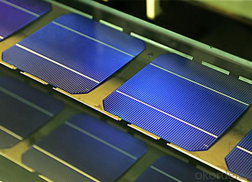


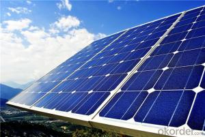
Multicrystalline Silicon Solar Wafer - High Quality A Grade Polycrystalline 5V 17.8% Solar Cell
- Ref Price:
-

- Loading Port:
- Shanghai
- Payment Terms:
- TT OR LC
- Min Order Qty:
- 1000 pc
- Supply Capability:
- 100000 pc/month
OKorder Service Pledge
OKorder Financial Service
You Might Also Like


Specifications
hot sale solar cell
1.16.8%~18.25% high efficiency
2.100% checked quality
3.ISO9001/ISO14001/TUV/CE/UL
4.stable performance
We can offer you the best quality products and services, don't miss !
POLY6'(156*156)
Polycrystalline Silicon Solar cell
Physical Characteristics
Dimension: 156mm×156mm±0.5mm
Diagonal: 220mm±0.5mm
Thickness(Si): 200±20 μm
Front(-) Back(+)
Blue anti-reflecting coating (silicon nitride); Aluminum back surface field;
1.5mm wide bus bars; 2.0mm wide soldering pads;
Distance between bus bars: 51mm . Distance between bus bars :51mm .
Electrical Characteristics
Efficiency(%) | 18.00 | 17.80 | 17.60 | 17.40 | 17.20 | 16.80 | 16.60 | 16.40 | 16.20 | 16.00 | 15.80 | 15.60 |
Pmpp(W) | 4.33 | 4.29 | 4.24 | 4.19 | 4.14 | 4.09 | 4.04 | 3.99 | 3.94 | 3.90 | 3.86 | 3.82 |
Umpp(V) | 0.530 | 0.527 | 0.524 | 0.521 | 0.518 | 0.516 | 0.514 | 0.511 | 0.509 | 0.506 | 0.503 | 0.501 |
Impp(A) | 8.159 | 8.126 | 8.081 | 8.035 | 7.990 | 7.938 | 7.876 | 7.813 | 7.754 | 7.698 | 7.642 | 7.586 |
Uoc(V) | 0.633 | 0.631 | 0.628 | 0.625 | 0.623 | 0.620 | 0.618 | 0.617 | 0.615 | 0.613 | 0.611 | 0.609 |
Isc(A) | 8.709 | 8.677 | 8.629 | 8.578 | 8.531 | 8.478 | 8.419 | 8.356 | 8.289 | 8.220 | 8.151 | 8.083 |

MONO5'(125*125mm)165
Monocrystalline silicon solar cell
Physical Characteristics
Dimension: 125mm×125mm±0.5mm
Diagonal: 165mm±0.5mm
Thickness(Si): 200±20 μm
Front(-) Back(+)
Blue anti-reflecting coating(silicon nitride); Aluminum back surface field;
1.6mmwide bus bars; 2.5mm wide soldering pads;
Distance between bus bars: 61mm . Distance between bus bars :61mm .
Electrical Characteristics
Efficiency(%) | 19.40 | 19.20 | 19.00 | 18.80 | 18.60 | 18.40 | 18.20 | 18.00 | 17.80 | 17.60 | 17.40 | 17.20 |
Pmpp(W) | 2.97 | 2.94 | 2.91 | 2.88 | 2.85 | 2.82 | 2.79 | 2.76 | 2.73 | 2.70 | 2.67 | 2.62 |
Umpp(V) | 0.537 | 0.535 | 0.533 | 0.531 | 0.527 | 0.524 | 0.521 | 0.518 | 0.516 | 0.515 | 0.513 | 0.509 |
Impp(A) | 5.531 | 5.495 | 5.460 | 5.424 | 5.408 | 5.382 | 5.355 | 5.328 | 5.291 | 5.243 | 5.195 | 4.147 |
Uoc(V) | 0.637 | 0.637 | 0.636 | 0.635 | 0.633 | 0.630 | 0.629 | 0.629 | 0.628 | 0.626 | 0.626 | 0.625 |
Isc(A) | 5.888 | 5.876 | 5.862 | 5.848 | 5.839 | 5.826 | 5.809 | 5.791 | 5.779 | 5.756 | 5.293 | 5.144 |

FAQ:
Q:How can i get some sample?
A:Yes , if you want order ,sample is not a problem.
Q:How about your solar panel efficency?
A: Our product efficency around 17.25%~18.25%.
Q:What’s the certificate you have got?
A: we have overall product certificate of ISO9001/ISO14001/CE/TUV/UL
- Q: How does the electrical conductivity affect the efficiency of a solar silicon wafer?
- The electrical conductivity of a solar silicon wafer directly affects its efficiency. Higher electrical conductivity allows for better flow of electric current, enabling the efficient collection and transport of generated electricity. This leads to improved overall performance and higher conversion efficiency of the solar cell. Consequently, a solar silicon wafer with higher electrical conductivity will typically result in a more efficient solar panel.
- Q: What is the role of surface texturing on solar silicon wafers?
- The role of surface texturing on solar silicon wafers is to enhance light trapping and absorption, thereby increasing the efficiency of the solar cells. The textured surface helps to reduce the amount of light reflection and scattering, allowing more photons to be absorbed by the silicon material and converted into electricity.
- Q: What is the purpose of an encapsulant in a solar silicon wafer?
- The purpose of an encapsulant in a solar silicon wafer is to protect the wafer from moisture, dust, and other environmental factors, ensuring its long-term durability and performance. It also helps to enhance the efficiency of the solar cell by minimizing reflection and providing a smooth surface for better light absorption.
- Q: Can solar silicon wafers be used in other applications besides solar energy?
- Yes, solar silicon wafers can be used in other applications besides solar energy. They are also used in the production of semiconductors, integrated circuits, and various electronic devices. Additionally, they can be utilized in the manufacturing of sensors, batteries, and even medical devices.
- Q: Can solar silicon wafers be used in solar-powered recreational facilities?
- Yes, solar silicon wafers can be used in solar-powered recreational facilities. Solar silicon wafers are a key component of solar panels, which convert sunlight into electricity. By harnessing solar power, recreational facilities can become more sustainable and reduce their reliance on traditional energy sources. The solar panels made from silicon wafers can be installed on rooftops, parking lots, or open spaces within the facility to generate clean, renewable energy. This can power various amenities such as lighting, heating, cooling, or even charging stations for electric vehicles, making solar-powered recreational facilities environmentally friendly and cost-effective in the long run.
- Q: Can solar silicon wafers be used in floating solar panel installations?
- Yes, solar silicon wafers can be used in floating solar panel installations. Floating solar panels typically use photovoltaic technology, which relies on silicon wafers to convert sunlight into electricity. By using these wafers, floating solar panels can efficiently harness solar energy even on water bodies, making them a viable and innovative solution for renewable energy generation.
- Q: Are there any limitations to the size of solar silicon wafers that can be produced?
- Yes, there are limitations to the size of solar silicon wafers that can be produced. Currently, the industry standard for solar panels is based on silicon wafers that are typically 156mm x 156mm or 210mm x 210mm in size. These dimensions are determined by several factors, including the manufacturing process, material properties, and handling constraints. While larger wafers may offer advantages in terms of increased efficiency and reduced costs, their production and handling become more challenging. Additionally, the size of the wafers is also constrained by the size of the equipment used in solar panel manufacturing. However, ongoing research and technological advancements may lead to further increases in the size of solar silicon wafers in the future.
- Q: Can solar silicon wafers be used in solar-powered street lighting systems?
- Yes, solar silicon wafers can be used in solar-powered street lighting systems. These wafers are the key component in solar panels, which capture sunlight and convert it into electricity. Solar-powered street lighting systems rely on solar panels to generate electricity during the day, which is stored in batteries and used to power the streetlights at night. Therefore, solar silicon wafers play a crucial role in the functioning of solar-powered street lighting systems.
- Q: How are solar silicon wafers etched to enhance light absorption?
- Solar silicon wafers are etched to enhance light absorption by using a chemical process called texturization. In this process, a mixture of acids is applied to the surface of the wafers, which creates tiny pyramid-like structures. These structures help to scatter and trap light within the material, increasing the chances of its absorption. This etching technique, known as black silicon, significantly improves the efficiency of solar cells by maximizing light absorption and reducing reflection.
- Q: Can solar silicon wafers be used in solar-powered telecommunications?
- Yes, solar silicon wafers can be used in solar-powered telecommunications. These wafers are commonly used in the production of photovoltaic cells, which convert sunlight into electricity. Since solar-powered telecommunications systems rely on harnessing solar energy to power their operations, solar silicon wafers are an essential component in the generation of electricity from sunlight.
Send your message to us
Multicrystalline Silicon Solar Wafer - High Quality A Grade Polycrystalline 5V 17.8% Solar Cell
- Ref Price:
-
- Loading Port:
- Shanghai
- Payment Terms:
- TT OR LC
- Min Order Qty:
- 1000 pc
- Supply Capability:
- 100000 pc/month
OKorder Service Pledge
OKorder Financial Service
Similar products


Hot products


Hot Searches
Related keywords

