


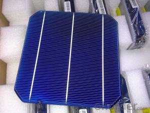
Mono Silicon Solar Wafer - 156mm*156mm Mono Solar Cells in Bulk Quantity Low Price Stock 18.0
- Ref Price:
-

- Loading Port:
- Shanghai
- Payment Terms:
- TT OR LC
- Min Order Qty:
- 1000 pc
- Supply Capability:
- 100000 pc/month
OKorder Service Pledge
OKorder Financial Service
You Might Also Like


Brief Introduction
- Up to 20.0% efficiency, one of the highest performing mono crystalline cells on the market
- Three bus bars boosts current collection over the entire cell area, leading to higher fill factors
- Blue anti-reflecting coating allows more sunlight be captured and converted to electricity
- Finer, closer fingers improves charge collections for improved energy yield
- Lower light-induced degradation leads to greater power output over the entire module lifetime
- All solar cells are tightly classified to optimize output of module
- Maximum yield and longevity due to hotspot prevention
- Premium appearance results in a highly uniform and aesthetically appealing module
Specification
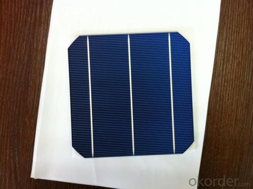
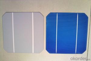
- Product Mono-crystalline silicon solar cell
- Dimension 156 mm x 156 mm ± 0.5 mm
- Thickness 200 μm ± 30 μm
- Front 1.5 ± 0.1 mm busbar (silver)
- Silicon nitride antireflection coating
- Back 3.0 mm continuous soldering pads (silver)
- Back surface field (aluminum)
Electric performance parameters

- Testing conditions: 1000 W/m2, AM 1.5, 25 °C, Tolerance: Efficiency ± 0.2% abs., Pmpp ±1.5% rel.
- Imin : at 0.5 V
Light Intensity Dependence

Soldering Ability
- Peel Strength: > 1.0 N/mm (Pull soldered ribbon from busbar in 5 mm/s of 180°)
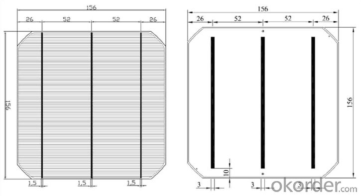
Dimension Figure

Quick Response
- Any time and anywhere, reply clients' email and solve all problems happen in the work at the first time.
- Remove clients doubts and offer the best solution at the first time.
- Give our clients the lastest news of the photovoltaic, update the newest stock informtion.
Production and Quality Control
- Precision cell efficiency sorting procedures
- Stringent criteria for color uniformity and appearance
- Reverse current and shunt resistance screening
- ISO9001,ISO14001 and OHSAS 18001,TUV Certificated


FAQ:
1. Q: Do you have your own factory?
A: Yes, we have. Our factory located in Jiangsu
2. Q: How can I visit your factory?
A: Before you visit,please contact us.We will show you the route or arrange a car to pick you up.
3. Q: Do you provide free sample?
A: Commenly we provide paid sample.
4. Q: Could you print our company LOGO on the nameplate and package?
A: Yes, we accept it.And need an Authorization Letter from you.
5. Q: Do you accept custom design on size?
A: Yes, if the size is reasonable.
6. Q: How can I be your agent in my country?
A: Please leave feedback. It's better for us to talk about details by email.
7. Q: Do you have solar project engineer who can guide me to install system?
A: Yes, we have a professional engineer team. They can teach you how to install a solar system.
- Q: How are solar silicon wafers tested for resistivity and sheet resistance?
- Solar silicon wafers are typically tested for resistivity and sheet resistance using a four-point probe technique. This involves using four evenly spaced probes to measure the resistance between each probe pair on the surface of the wafer. By applying a known current and measuring the voltage drop, resistivity and sheet resistance can be calculated using established mathematical formulas.
- Q: Can solar silicon wafers be used in solar-powered space vehicles?
- Yes, solar silicon wafers can be used in solar-powered space vehicles. Solar silicon wafers are commonly used in photovoltaic systems to convert sunlight into electricity. In space, where there is abundant sunlight, solar panels made with silicon wafers can efficiently capture and convert solar energy into electrical power to operate various systems and equipment onboard the space vehicles.
- Q: How is a glass cover attached to a solar silicon wafer?
- A glass cover is typically attached to a solar silicon wafer using a combination of adhesive materials and a lamination process. The wafer is first coated with a thin layer of adhesive, and then the glass cover is carefully placed on top. Pressure and heat are then applied to initiate the lamination process, which helps to create a strong bond between the glass cover and the wafer. This bonding process ensures that the solar cells are protected from external factors such as dust, moisture, and physical damage.
- Q: What is a good solar wafer testing equipment?
- PL-- detection of micro cracks, black spots, black and other issuesWafer sorting - Detection AOI, PN, resistivity, thickness, lifetime, stria depth
- Q: How do solar silicon wafers contribute to the electrification of remote areas?
- Solar silicon wafers contribute to the electrification of remote areas by being the primary component of solar panels. These panels harness solar energy and convert it into electricity, providing a sustainable and renewable source of power. In remote areas where traditional electricity grids are absent or unreliable, solar panels with silicon wafers can be deployed to generate clean energy and bring electricity to communities that would otherwise be without it.
- Q: How is the surface of a solar silicon wafer textured?
- The surface of a solar silicon wafer is textured by using various techniques such as acid etching or laser ablation. These methods create a pattern of tiny pyramidal or needle-like structures on the surface, which helps to trap and scatter light, increasing the absorption efficiency of the silicon wafer.
- Q: What are the potential future advancements in solar silicon wafer technology?
- Some potential future advancements in solar silicon wafer technology include increasing the efficiency of solar cells by developing new manufacturing techniques, such as nanostructuring or using tandem solar cells. There is also ongoing research to reduce costs by improving the production process and exploring alternative materials for solar cells, such as perovskites. Additionally, advancements in silicon wafer technology may include the development of flexible or transparent solar cells, allowing for integration into various surfaces and applications.
- Q: What is the typical lead time for ordering solar silicon wafers?
- The typical lead time for ordering solar silicon wafers can range from a few weeks to a few months, depending on various factors such as supplier availability, order quantity, and customization requirements. It is recommended to check with the specific supplier or manufacturer to get an accurate estimate for the lead time.
- Q: How do solar silicon wafers perform in dusty environments?
- Solar silicon wafers can experience reduced performance in dusty environments due to the accumulation of dust particles on their surface. Dust can block sunlight and create a barrier between the wafer and the sunlight it needs to generate electricity. This can lead to a decrease in the efficiency of solar panels and a reduction in their overall power output. Regular cleaning and maintenance of solar panels in dusty environments is essential to ensure optimal performance.
- Q: What are some of the silicon wafer factory
- 2 raw materials for deputy director, assistant director of the workshop material sorting and packaging materials packaging materials sorting operator monitor corrosion monitor cleaning cleaning raw materials warehousing operator member subtotal deputy director of the 3 crystal sandblasting operator workshop director assistant assistant statistician crystal crystal pulling monitor operator cut cut monitor operator subtotal
Send your message to us
Mono Silicon Solar Wafer - 156mm*156mm Mono Solar Cells in Bulk Quantity Low Price Stock 18.0
- Ref Price:
-
- Loading Port:
- Shanghai
- Payment Terms:
- TT OR LC
- Min Order Qty:
- 1000 pc
- Supply Capability:
- 100000 pc/month
OKorder Service Pledge
OKorder Financial Service
Similar products


Hot products


Hot Searches
Related keywords

