


Solar Silicon Wafer Mono Solar Cells 156mm*156mm in Bulk Quantity Low Price Stock 18.4
- Ref Price:
-

- Loading Port:
- Shanghai
- Payment Terms:
- TT OR LC
- Min Order Qty:
- 1000 pc
- Supply Capability:
- 100000 pc/month
OKorder Service Pledge
OKorder Financial Service
You Might Also Like


Brief Introduction
- Up to 20.0% efficiency, one of the highest performing mono crystalline cells on the market
- Three bus bars boosts current collection over the entire cell area, leading to higher fill factors
- Blue anti-reflecting coating allows more sunlight be captured and converted to electricity
- Finer, closer fingers improves charge collections for improved energy yield
- Lower light-induced degradation leads to greater power output over the entire module lifetime
- All solar cells are tightly classified to optimize output of module
- Maximum yield and longevity due to hotspot prevention
- Premium appearance results in a highly uniform and aesthetically appealing module
Specification
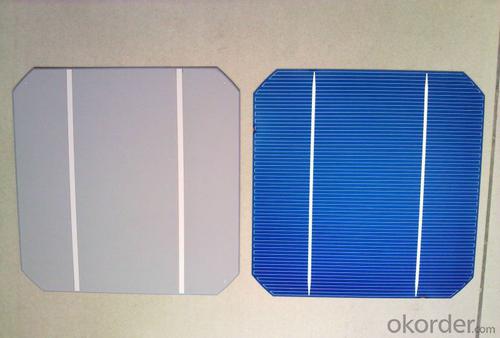
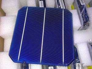
- Product Mono-crystalline silicon solar cell
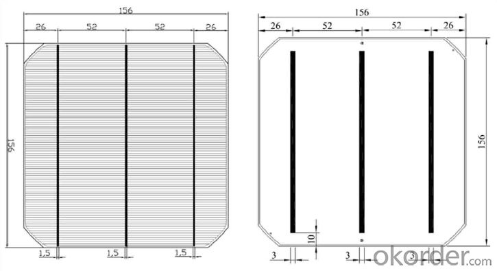
- Dimension 156 mm x 156 mm ± 0.5 mm
- Thickness 200 μm ± 30 μm
- Front 1.5 ± 0.1 mm busbar (silver)
- Silicon nitride antireflection coating
- Back 3.0 mm continuous soldering pads (silver)
- Back surface field (aluminum)
Electric performance parameters

- Testing conditions: 1000 W/m2, AM 1.5, 25 °C, Tolerance: Efficiency ± 0.2% abs., Pmpp ±1.5% rel.
- Imin : at 0.5 V
Light Intensity Dependence

Soldering Ability
- Peel Strength: > 1.0 N/mm (Pull soldered ribbon from busbar in 5 mm/s of 180°)
Dimension Figure

Quick Response
- Any time and anywhere, reply clients' email and solve all problems happen in the work at the first time.
- Remove clients doubts and offer the best solution at the first time.
- Give our clients the lastest news of the photovoltaic, update the newest stock informtion.
Production and Quality Control
- Precision cell efficiency sorting procedures
- Stringent criteria for color uniformity and appearance
- Reverse current and shunt resistance screening
- ISO9001,ISO14001 and OHSAS 18001,TUV Certificated


FAQ:
1. Q: Do you have your own factory?
A: Yes, we have. Our factory located in Jiangsu
2. Q: How can I visit your factory?
A: Before you visit,please contact us.We will show you the route or arrange a car to pick you up.
3. Q: Do you provide free sample?
A: Commenly we provide paid sample.
4. Q: Could you print our company LOGO on the nameplate and package?
A: Yes, we accept it.And need an Authorization Letter from you.
5. Q: Do you accept custom design on size?
A: Yes, if the size is reasonable.
6. Q: How can I be your agent in my country?
A: Please leave feedback. It's better for us to talk about details by email.
7. Q: Do you have solar project engineer who can guide me to install system?
A: Yes, we have a professional engineer team. They can teach you how to install a solar system.
- Q: What are the different surface texturing techniques used for solar silicon wafers?
- There are several surface texturing techniques used for solar silicon wafers, including acid etching, plasma etching, laser texturing, and chemical texturing. These techniques are employed to increase the light trapping efficiency of the wafers, enhance the absorption of sunlight, and improve the overall performance of solar cells.
- Q: The benefits of silicon chip
- (1) classification of silicon steel sheetA and silicon steel sheet can be divided into two kinds: low silicon and high silicon. Low silicon silicon containing less than 2.8%, it has a certain mechanical strength, mainly used in the manufacture of motor, commonly known as dynamosheet; high silicon silicon content is 2.8%-4.8%, it has good magnetic properties, but more brittle, mainly used in the manufacture of transformer core, commonly known as the transformer silicon steel sheet. There is no strict limit in the actual use, the use of large silicon wafer manufacturing large motor. B, according to production and processing process can be divided into two kinds of hot rolling and cold rolling, cold rolling can be divided into grain orientation and grain orientation of the two. Cold rolled sheet of uniform thickness, good surface quality, high magnetic, therefore, with the development of industry, the trend of hot rolled sheet is cold rolled sheet has replaced (China has explicitly requested to stop the use of hot rolled silicon steel sheet, which is called "pre cold generation of heat")
- Q: How are solar silicon wafers cleaned during the manufacturing process?
- Solar silicon wafers are cleaned during the manufacturing process through a multi-step procedure. Initially, the wafers are subjected to a chemical clean to remove any organic and inorganic impurities present on their surfaces. This involves using acid or alkaline solutions to dissolve and eliminate contaminants. Following the chemical clean, the wafers undergo a rinse process with deionized water to remove any remaining chemicals. Lastly, the wafers are dried using a combination of heat and air or a spin-dry technique to ensure a clean and dry surface before further processing.
- Q: What is the current industry standard for solar silicon wafer thickness?
- The current industry standard for solar silicon wafer thickness ranges from 180 to 200 micrometers.
- Q: The microprocessor integrates the computer with what is on a small silicon chip
- The controller (English Name: controller) is a master device in accordance with the resistance change circuit wiring and a predetermined sequence change or control circuit to control the value of motor starting, speed control, braking and reverse.It consists of the program counter, the instruction register, the instruction decoder, the timing generator and the operation controller. It is the "decision making mechanism", which is to coordinate and direct the operation of the whole computer system.
- Q: Why do monocrystalline silicon chamfer? Polysilicon film?
- Chamfering is for this purpose, grinding and polishing are also for this purpose. As a single crystal practitioners, it is recommended that you take a look at the processing technology of silicon single crystal wafer > this book, written by Zhang Juezong, more comprehensive
- Q: How are solar silicon wafers disposed of at the end of their life cycle?
- Solar silicon wafers are typically recycled at the end of their life cycle. Various recycling methods are employed, including mechanical and chemical processes, to separate and recover valuable materials such as silicon, silver, and glass. These recovered materials can then be reused in the manufacturing of new solar panels or other products, minimizing waste and reducing the environmental impact of the solar industry.
- Q: How are solar silicon wafers affected by light trapping techniques?
- Solar silicon wafers are positively influenced by light trapping techniques as these methods improve the absorption of light within the wafer, thereby enhancing its overall efficiency in converting sunlight into electricity. Light trapping techniques, such as texturing the surface or adding anti-reflective coatings, help to increase the path length of light within the wafer, ensuring that more photons are absorbed and utilized. This results in higher power output and improved performance of solar cells using silicon wafers.
- Q: How are solar silicon wafers tested for electrical properties?
- Solar silicon wafers are typically tested for their electrical properties using a variety of techniques. One common method is known as the four-point probe measurement, in which four probes are placed on the surface of the wafer to measure its resistivity. This test helps determine the quality and purity of the silicon material. Additionally, the wafers may undergo tests such as the dark current-voltage (IV) measurement, which provides information about the electrical behavior in the absence of light, and the light IV measurement, which analyzes the performance of the wafer under illumination. These tests help assess the efficiency and overall electrical characteristics of the solar silicon wafers.
- Q: What is the impact of impurity concentration on solar silicon wafers?
- The impurity concentration in solar silicon wafers has a significant impact on their performance and efficiency. Higher impurity concentrations can lead to reduced electrical conductivity, decreased carrier lifetime, and increased recombination, all of which can negatively affect the overall efficiency of the solar cell. Impurities such as iron, copper, and chromium can act as recombination centers, causing a loss of photo-generated carriers. Therefore, minimizing impurity concentration is crucial in order to maximize the efficiency and performance of solar silicon wafers.
Send your message to us
Solar Silicon Wafer Mono Solar Cells 156mm*156mm in Bulk Quantity Low Price Stock 18.4
- Ref Price:
-
- Loading Port:
- Shanghai
- Payment Terms:
- TT OR LC
- Min Order Qty:
- 1000 pc
- Supply Capability:
- 100000 pc/month
OKorder Service Pledge
OKorder Financial Service
Similar products


Hot products


Hot Searches
Related keywords

