


Ic Grade Solar Silicon Wafer Supplier - High Quality A Grade Mono Crystalline 5V 17.8% Solar Cell
- Ref Price:
-

- Loading Port:
- Shanghai
- Payment Terms:
- TT OR LC
- Min Order Qty:
- 1000 pc
- Supply Capability:
- 100000 pc/month
OKorder Service Pledge
OKorder Financial Service
You Might Also Like


Specifications
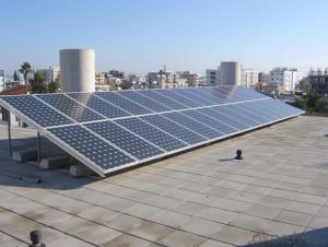
hot sale solar cell
1.16.8%~18.25% high efficiency
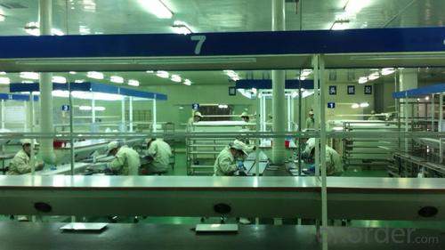
2.100% checked quality
3.ISO9001/ISO14001/TUV/CE/UL
4.stable performance
We can offer you the best quality products and services, don't miss !
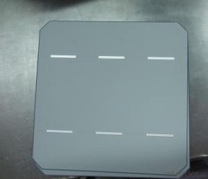
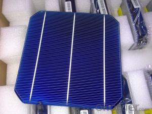
POLY6'(156*156)
Polycrystalline Silicon Solar cell
Physical Characteristics
Dimension: 156mm×156mm±0.5mm
Diagonal: 220mm±0.5mm
Thickness(Si): 200±20 μm
Front(-) Back(+)
Blue anti-reflecting coating (silicon nitride); Aluminum back surface field;
1.5mm wide bus bars; 2.0mm wide soldering pads;
Distance between bus bars: 51mm . Distance between bus bars :51mm .
Electrical Characteristics
Efficiency(%) | 18.00 | 17.80 | 17.60 | 17.40 | 17.20 | 16.80 | 16.60 | 16.40 | 16.20 | 16.00 | 15.80 | 15.60 |
Pmpp(W) | 4.33 | 4.29 | 4.24 | 4.19 | 4.14 | 4.09 | 4.04 | 3.99 | 3.94 | 3.90 | 3.86 | 3.82 |
Umpp(V) | 0.530 | 0.527 | 0.524 | 0.521 | 0.518 | 0.516 | 0.514 | 0.511 | 0.509 | 0.506 | 0.503 | 0.501 |
Impp(A) | 8.159 | 8.126 | 8.081 | 8.035 | 7.990 | 7.938 | 7.876 | 7.813 | 7.754 | 7.698 | 7.642 | 7.586 |
Uoc(V) | 0.633 | 0.631 | 0.628 | 0.625 | 0.623 | 0.620 | 0.618 | 0.617 | 0.615 | 0.613 | 0.611 | 0.609 |
Isc(A) | 8.709 | 8.677 | 8.629 | 8.578 | 8.531 | 8.478 | 8.419 | 8.356 | 8.289 | 8.220 | 8.151 | 8.083 |

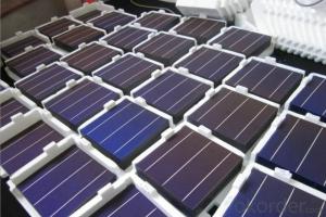
MONO5'(125*125mm)165
Monocrystalline silicon solar cell
Physical Characteristics
Dimension: 125mm×125mm±0.5mm
Diagonal: 165mm±0.5mm
Thickness(Si): 200±20 μm
Front(-) Back(+)
Blue anti-reflecting coating(silicon nitride); Aluminum back surface field;
1.6mmwide bus bars; 2.5mm wide soldering pads;
Distance between bus bars: 61mm . Distance between bus bars :61mm .
Electrical Characteristics
Efficiency(%) | 19.40 | 19.20 | 19.00 | 18.80 | 18.60 | 18.40 | 18.20 | 18.00 | 17.80 | 17.60 | 17.40 | 17.20 |
Pmpp(W) | 2.97 | 2.94 | 2.91 | 2.88 | 2.85 | 2.82 | 2.79 | 2.76 | 2.73 | 2.70 | 2.67 | 2.62 |
Umpp(V) | 0.537 | 0.535 | 0.533 | 0.531 | 0.527 | 0.524 | 0.521 | 0.518 | 0.516 | 0.515 | 0.513 | 0.509 |
Impp(A) | 5.531 | 5.495 | 5.460 | 5.424 | 5.408 | 5.382 | 5.355 | 5.328 | 5.291 | 5.243 | 5.195 | 4.147 |
Uoc(V) | 0.637 | 0.637 | 0.636 | 0.635 | 0.633 | 0.630 | 0.629 | 0.629 | 0.628 | 0.626 | 0.626 | 0.625 |
Isc(A) | 5.888 | 5.876 | 5.862 | 5.848 | 5.839 | 5.826 | 5.809 | 5.791 | 5.779 | 5.756 | 5.293 | 5.144 |

FAQ:
Q:How can i get some sample?
A:Yes , if you want order ,sample is not a problem.
Q:How about your solar panel efficency?
A: Our product efficency around 17.25%~18.25%.
Q:What’s the certificate you have got?
A: we have overall product certificate of ISO9001/ISO14001/CE/TUV/UL
- Q: What is the role of a bypass diode in a solar silicon wafer?
- The role of a bypass diode in a solar silicon wafer is to provide an alternative current path when a portion of the wafer is shaded or damaged. It helps prevent power losses by bypassing the shaded or damaged section, allowing the unaffected sections to continue generating electricity efficiently.
- Q: What is the expected future development of solar silicon wafers?
- The expected future development of solar silicon wafers involves advancements in efficiency, cost reduction, and increased sustainability. Technological innovations like thinner wafers, improved manufacturing processes, and the integration of novel materials are likely to enhance the efficiency of solar cells. Additionally, the use of advanced manufacturing techniques such as heterojunction technology and passivated emitter rear contact (PERC) technology is expected to further improve the performance of solar silicon wafers. Furthermore, research efforts are focused on developing sustainable and environmentally friendly methods for silicon production, such as recycling and utilizing lower-grade silicon sources. Overall, the future holds great potential for solar silicon wafers to become more efficient, cost-effective, and eco-friendly, thereby contributing to the widespread adoption of solar energy.
- Q: What is the typical warranty period for a solar silicon wafer?
- The typical warranty period for a solar silicon wafer can vary depending on the manufacturer, but it is commonly around 25 to 30 years.
- Q: What is the role of the back contact on a solar silicon wafer?
- The role of the back contact on a solar silicon wafer is to provide electrical contact to the bottom layer of the solar cell. This contact allows for the collection and extraction of the generated electrical current, ensuring efficient energy conversion. Additionally, the back contact also acts as a reflective surface, enhancing light absorption and reducing energy loss in the solar cell.
- Q: What is a silicon wafer cutting edge material?
- Because the cutting edge material particles have very sharp edges, and the hardness is far greater than the silicon rod or silicon ingot hardness, so the silicon rod or silicon ingot and steel wire contact area gradually by the cutting edge material particle grinding off, so as to achieve the purpose of cutting.
- Q: How does the efficiency of a solar silicon wafer change with humidity?
- The efficiency of a solar silicon wafer generally decreases with increasing humidity. High humidity levels can cause moisture to accumulate on the surface of the wafer, leading to a decrease in the wafer's ability to convert sunlight into electricity. This moisture can create a barrier that reduces the amount of light reaching the semiconductor material, thereby reducing the overall efficiency of the solar cell. Furthermore, humidity can also affect the electrical properties of the silicon material, leading to increased resistance and decreased performance. Therefore, it is important to consider humidity levels when evaluating the efficiency of a solar silicon wafer.
- Q: How is the power output of a solar silicon wafer measured?
- The power output of a solar silicon wafer is typically measured by exposing it to a known intensity of light and recording the current and voltage produced. This measurement is conducted using a device called a solar cell tester or solar simulator, which simulates sunlight and provides accurate readings of the wafer's power output.
- Q: What are the disadvantages of using a solar silicon wafer in solar cells?
- One of the main disadvantages of using a solar silicon wafer in solar cells is its high production cost. Silicon wafers require a complex and energy-intensive manufacturing process, which adds to the overall cost of producing solar cells. Additionally, silicon wafers are rigid and brittle, making them prone to damage during handling and installation. This fragility can lead to higher maintenance and replacement costs. Moreover, silicon wafers have a lower efficiency in converting sunlight into electricity compared to other materials, such as thin-film solar cells. This lower efficiency means that larger surface areas are required to generate the same amount of power, resulting in increased material usage and cost.
- Q: Below what the photovoltaic industry specific industry classification, solar silicon manufacturing enterprises, mainly engaged in single and polycrystalline silicon, polycrystalline silicon wafer cutting casting, single enterprise, what are the concrete classification, a solar silicon slice of this industry?
- Polysilicon for chemical, silicon wafer for machining, battery components for semiconductor processing
- Q: How are defects in solar silicon wafers detected?
- Defects in solar silicon wafers are detected through various methods, including visual inspection, electrical testing, and imaging techniques. Visual inspection involves examining the surface of the wafer for any visible imperfections or irregularities. Electrical testing measures the electrical characteristics of the wafer, such as its resistivity and efficiency, to identify any deviations from the desired specifications. Imaging techniques such as infrared thermography or photoluminescence imaging can also be used to detect defects by capturing images that reveal anomalies or inconsistencies in the wafer's structure or composition.
Send your message to us
Ic Grade Solar Silicon Wafer Supplier - High Quality A Grade Mono Crystalline 5V 17.8% Solar Cell
- Ref Price:
-
- Loading Port:
- Shanghai
- Payment Terms:
- TT OR LC
- Min Order Qty:
- 1000 pc
- Supply Capability:
- 100000 pc/month
OKorder Service Pledge
OKorder Financial Service
Similar products


Hot products


Hot Searches
Related keywords

