


High Current Monocrystalline Solar Silicon Wafer 17.6% Polycrystalline Silicon Solar Cell Price
- Ref Price:
-

- Loading Port:
- Shanghai
- Payment Terms:
- TT OR LC
- Min Order Qty:
- 1000 pc
- Supply Capability:
- 100000 pc/month
OKorder Service Pledge
OKorder Financial Service
You Might Also Like


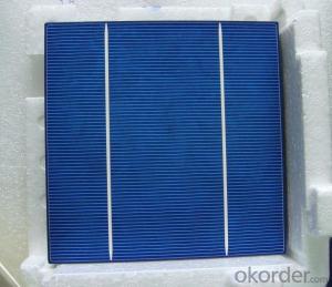
4 Bus Bars 156*156 17.6% efficiency poly solar cell
PHYSICAL CHARACTERISTICS
Dimension: 156mm x 156mm ± 0.5mm
Wafer Thickeness: 180um+20um and 200um+20um
Front(-) Four 1.2mm silver busbar
Silicon nitride blue anti-reflection coating
Back(+) aluminum back surface field
1.75mm(silver) wide segment soldering pads

Typical Electrical Characteristics
Efficiency | W(Pmpp) | V(Umpp) | A(Impp) | V(Uoc) | A(Isc) |
17.4-17.5 | 4.234 | 0.517 | 8.231 | 0.622 | 8.759 |
17.5-17.6 | 4.259 | 0.519 | 8.243 | 0.623 | 8.769 |
17.7-17.8 | 4.283 | 0.521 | 8.256 | 0.625 | 8.779 |
17.8-17.9 | 4.307 | 0.523 | 8.268 | 0.626 | 8.788 |
17.9-18.0 | 4.332 | 0.525 | 8.281 | 0.627 | 8.798 |
18.0-18.1 | 4.380 | 0.529 | 8.306 | 0.629 | 8.808 |
18.1-18.2 | 4.405 | 0.531 | 8.318 | 0.632 | 8.818 |
18.2-18.3 | 4.429 | 0.533 | 8.331 | 0.633 | 8.837 |
18.3-18.4 | 4.453 | 0.535 | 8.344 | 0.634 | 8.847 |
18.4-18.5 | 4.478 | 0.537 | 8.356 | 0.636 | 8.856 |
18.5-18.6 | 4.502 | 0.539 | 8.369 | 0.637 | 8.866 |
Efficiency | W(Pmpp) | V(Umpp) | A(Impp) | V(Uoc) | A(Isc) |
20.90-21.00 | 5.06 | 0.557 | 9.007 | 0.653 | 9.688 |
20.80-20.90 | 5.04 | 0.556 | 9.062 | 0.652 | 9.683 |
20.70-20.80 | 5.02 | 0.554 | 9.055 | 0.651 | 9.684 |
20.60-20.70 | 4.99 | 0.552 | 9.033 | 0.651 | 9.672 |
20.50-20.60 | 4.97 | 0.550 | 9.002 | 0.650 | 9.673 |
20.40-20.50 | 4.94 | 0.548 | 9.012 | 0.649 | 9.674 |
20.30-20.40 | 4.92 | 0.546 | 9.009 | 0.649 | 9.655 |
20.20-20.30 | 4.89 | 0.543 | 9.012 | 0.648 | 9.634 |
20.10-20.20 | 4.87 | 0.541 | 8.998 | 0.648 | 9.617 |
20.00-20.10 | 4.85 | 0.540 | 8.977 | 0.647 | 9.600 |
*Data under standard testing conditional (STC):1,000w/m2,AM1.5, 25°C , Pmax:Positive power tolerance.
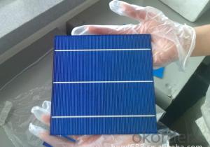
3 Bus Bars 156*156 17.4% efficiency poly solar cell
Dimension: 156 mm x 156 mm ± 0.5 mm
Wafer Thickeness: 156 mm x 156 mm ± 0.5 mm

Typical Electrical Characteristics:
| Efficiency code | 1660 | 1680 | 1700 | 1720 | 1740 | 1760 | 1780 | 1800 | 1820 | 1840 | 1860 |
| Efficiency (%) | 16.6 | 16.8 | 17.0 | 17.2 | 17.4 | 17.6 | 17.8 | 18.0 | 18.2 | 18.4 | 18.6 |
| Pmax (W) | 4.04 | 4.09 | 4.14 | 4.19 | 4.23 | 4.28 | 4.33 | 4.38 | 4.43 | 4.48 | 4.53 |
| Voc (V) | 0.612 | 0.615 | 0.618 | 0.621 | 0.624 | 0.627 | 0.629 | 0.63 | 0.633 | 0.635 | 0.637 |
| Isc (A) | 8.42 | 8.46 | 8.51 | 8.56 | 8.61 | 8.65 | 8.69 | 8.73 | 8.77 | 8.81 | 8.84 |
| Imp (A) | 7.91 | 7.99 | 8.08 | 8.16 | 8.22 | 8.27 | 8.33 | 8.38 | 8.43 | 8.48 | 8.53 |
* Testing conditions: 1000 W/m2, AM 1.5, 25 °C, Tolerance: Efficiency ± 0.2% abs., Pmpp ±1.5% rel.
* Imin : at 0.5 V
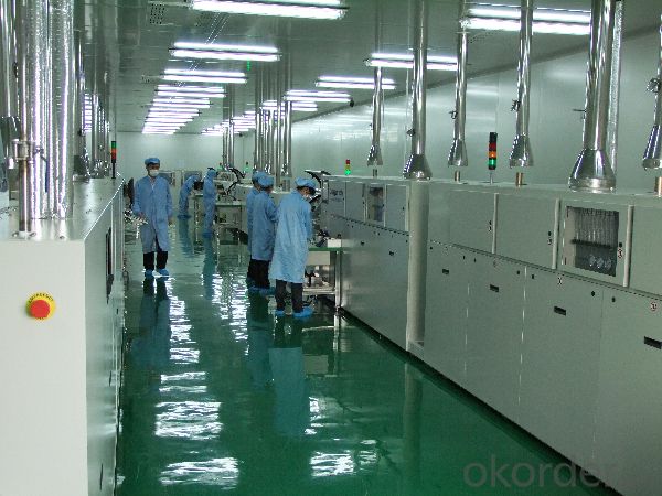
Production:

Package:

FAQ:
1. Q: Do you have your own factory?
A: Yes, we have. Our factory located in Jiangsu
2. Q: How can I visit your factory?
A: Before you visit,please contact us.We will show you the route or arrange a car to pick you up.
3. Q: Do you provide free sample?
A: Commenly we provide paid sample.
4. Q: Could you print our company LOGO on the nameplate and package?
A: Yes, we accept it.And need an Authorization Letter from you.
5. Q: Do you accept custom design on size?
A: Yes, if the size is reasonable.
6. Q: How can I be your agent in my country?
A: Please leave feedback. It's better for us to talk about details by email.
7. Q: Do you have solar project engineer who can guide me to install system?
A: Yes, we have a professional engineer team. They can teach you how to install a solar system.
- Q: How does the texturing process affect the performance of a solar silicon wafer?
- The texturing process plays a crucial role in enhancing the performance of a solar silicon wafer. By creating a textured surface, the surface area of the wafer increases, allowing for better light absorption. This increased absorption enables the wafer to capture more sunlight, resulting in higher energy conversion efficiency. Additionally, the texturing process helps to reduce the reflection of sunlight, minimizing the loss of incoming light energy. Overall, the texturing process significantly improves the performance of a solar silicon wafer by maximizing light absorption and minimizing energy loss.
- Q: Can solar silicon wafers be used in solar-powered remote sensing devices?
- Yes, solar silicon wafers can be used in solar-powered remote sensing devices. These wafers are commonly used in solar panels to convert sunlight into electrical energy, making them suitable for powering various remote sensing devices that require energy-efficient and sustainable power sources.
- Q: Can solar silicon wafers be used in solar-powered irrigation systems?
- Yes, solar silicon wafers can be used in solar-powered irrigation systems. These wafers are commonly used in solar panels to convert sunlight into electricity, which can then be utilized to power irrigation systems. By harnessing solar energy, these systems provide a sustainable and renewable source of power for irrigation, reducing reliance on traditional electricity sources and promoting eco-friendly farming practices.
- Q: How is a mounting structure attached to a solar silicon wafer?
- A mounting structure is typically attached to a solar silicon wafer using a conductive adhesive or soldering technique. The adhesive or solder is applied to the backside of the wafer, and the mounting structure is then pressed onto it. This ensures a secure and reliable connection between the wafer and the mounting structure, enabling the efficient installation and operation of the solar panel.
- Q: Can solar silicon wafers be used in underwater applications?
- No, solar silicon wafers cannot be used in underwater applications as they are not designed to withstand the harsh conditions and pressure underwater.
- Q: What is the average lifespan of a solar silicon wafer?
- The average lifespan of a solar silicon wafer can vary depending on various factors such as the manufacturing quality, usage conditions, and maintenance practices. However, on average, a well-maintained and properly used solar silicon wafer can last for around 25 to 30 years.
- Q: What is the expected efficiency improvement for multi-junction perovskite-silicon solar silicon wafers?
- The expected efficiency improvement for multi-junction perovskite-silicon solar silicon wafers is significant. With the combination of perovskite and silicon materials, these solar cells can potentially achieve higher efficiencies due to their ability to capture a broader range of the solar spectrum. This enables them to convert a larger portion of sunlight into electricity, leading to improved overall efficiency compared to traditional silicon-based solar cells. However, the exact improvement in efficiency would depend on various factors such as the specific materials used, the device architecture, and ongoing research and development efforts in this field.
- Q: Can solar silicon wafers be used in wearable fashion accessories?
- Yes, solar silicon wafers can be used in wearable fashion accessories. The small size and flexibility of these wafers make them suitable for integrating into accessories like smartwatches, bracelets, or even clothing items. By harnessing solar energy, these accessories can power various functionalities, such as charging small electronic devices or monitoring health metrics. Additionally, the use of solar silicon wafers aligns with the growing trend of sustainable fashion, making them an attractive option for eco-conscious consumers.
- Q: What is the typical shelf life of a solar silicon wafer?
- The typical shelf life of a solar silicon wafer can vary, but it is generally considered to be around 1-2 years.
- Q: Can solar silicon wafers be used in solar-powered telecommunications?
- Yes, solar silicon wafers can be used in solar-powered telecommunications. These wafers are commonly used in the production of photovoltaic cells, which convert sunlight into electricity. Since solar-powered telecommunications systems rely on harnessing solar energy to power their operations, solar silicon wafers are an essential component in the generation of electricity from sunlight.
Send your message to us
High Current Monocrystalline Solar Silicon Wafer 17.6% Polycrystalline Silicon Solar Cell Price
- Ref Price:
-
- Loading Port:
- Shanghai
- Payment Terms:
- TT OR LC
- Min Order Qty:
- 1000 pc
- Supply Capability:
- 100000 pc/month
OKorder Service Pledge
OKorder Financial Service
Similar products


Hot products


Hot Searches
Related keywords

