


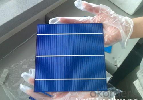

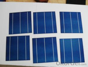
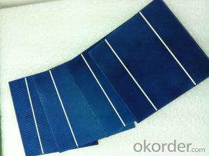
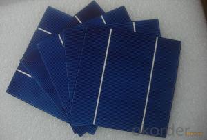
Silicon Wafer Based High Current 17.4% Polycrystalline Silicon Solar Cells
- Ref Price:
-

- Loading Port:
- Shanghai
- Payment Terms:
- TT OR LC
- Min Order Qty:
- 1000 pc
- Supply Capability:
- 100000 pc/month
OKorder Service Pledge
OKorder Financial Service
You Might Also Like


4 Bus Bars 156*156 17.6% efficiency poly solar cell
PHYSICAL CHARACTERISTICS
Dimension: 156mm x 156mm ± 0.5mm
Wafer Thickeness: 180um+20um and 200um+20um
Front(-) Four 1.2mm silver busbar
Silicon nitride blue anti-reflection coating
Back(+) aluminum back surface field
1.75mm(silver) wide segment soldering pads

Typical Electrical Characteristics
Efficiency | W(Pmpp) | V(Umpp) | A(Impp) | V(Uoc) | A(Isc) |
17.4-17.5 | 4.234 | 0.517 | 8.231 | 0.622 | 8.759 |
17.5-17.6 | 4.259 | 0.519 | 8.243 | 0.623 | 8.769 |
17.7-17.8 | 4.283 | 0.521 | 8.256 | 0.625 | 8.779 |
17.8-17.9 | 4.307 | 0.523 | 8.268 | 0.626 | 8.788 |
17.9-18.0 | 4.332 | 0.525 | 8.281 | 0.627 | 8.798 |
18.0-18.1 | 4.380 | 0.529 | 8.306 | 0.629 | 8.808 |
18.1-18.2 | 4.405 | 0.531 | 8.318 | 0.632 | 8.818 |
18.2-18.3 | 4.429 | 0.533 | 8.331 | 0.633 | 8.837 |
18.3-18.4 | 4.453 | 0.535 | 8.344 | 0.634 | 8.847 |
18.4-18.5 | 4.478 | 0.537 | 8.356 | 0.636 | 8.856 |
18.5-18.6 | 4.502 | 0.539 | 8.369 | 0.637 | 8.866 |
Efficiency | W(Pmpp) | V(Umpp) | A(Impp) | V(Uoc) | A(Isc) |
20.90-21.00 | 5.06 | 0.557 | 9.007 | 0.653 | 9.688 |
20.80-20.90 | 5.04 | 0.556 | 9.062 | 0.652 | 9.683 |
20.70-20.80 | 5.02 | 0.554 | 9.055 | 0.651 | 9.684 |
20.60-20.70 | 4.99 | 0.552 | 9.033 | 0.651 | 9.672 |
20.50-20.60 | 4.97 | 0.550 | 9.002 | 0.650 | 9.673 |
20.40-20.50 | 4.94 | 0.548 | 9.012 | 0.649 | 9.674 |
20.30-20.40 | 4.92 | 0.546 | 9.009 | 0.649 | 9.655 |
20.20-20.30 | 4.89 | 0.543 | 9.012 | 0.648 | 9.634 |
20.10-20.20 | 4.87 | 0.541 | 8.998 | 0.648 | 9.617 |
20.00-20.10 | 4.85 | 0.540 | 8.977 | 0.647 | 9.600 |
*Data under standard testing conditional (STC):1,000w/m2,AM1.5, 25°C , Pmax:Positive power tolerance.
3 Bus Bars 156*156 17.4% efficiency poly solar cell
Dimension: 156 mm x 156 mm ± 0.5 mm
Wafer Thickeness: 156 mm x 156 mm ± 0.5 mm

Typical Electrical Characteristics:
| Efficiency code | 1660 | 1680 | 1700 | 1720 | 1740 | 1760 | 1780 | 1800 | 1820 | 1840 | 1860 |
| Efficiency (%) | 16.6 | 16.8 | 17.0 | 17.2 | 17.4 | 17.6 | 17.8 | 18.0 | 18.2 | 18.4 | 18.6 |
| Pmax (W) | 4.04 | 4.09 | 4.14 | 4.19 | 4.23 | 4.28 | 4.33 | 4.38 | 4.43 | 4.48 | 4.53 |
| Voc (V) | 0.612 | 0.615 | 0.618 | 0.621 | 0.624 | 0.627 | 0.629 | 0.63 | 0.633 | 0.635 | 0.637 |
| Isc (A) | 8.42 | 8.46 | 8.51 | 8.56 | 8.61 | 8.65 | 8.69 | 8.73 | 8.77 | 8.81 | 8.84 |
| Imp (A) | 7.91 | 7.99 | 8.08 | 8.16 | 8.22 | 8.27 | 8.33 | 8.38 | 8.43 | 8.48 | 8.53 |
* Testing conditions: 1000 W/m2, AM 1.5, 25 °C, Tolerance: Efficiency ± 0.2% abs., Pmpp ±1.5% rel.
* Imin : at 0.5 V
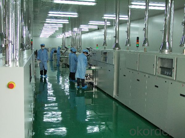
Production:

Package:

FAQ:
1. Q: Do you have your own factory?
A: Yes, we have. Our factory located in Jiangsu
2. Q: How can I visit your factory?
A: Before you visit,please contact us.We will show you the route or arrange a car to pick you up.
3. Q: Do you provide free sample?
A: Commenly we provide paid sample.
4. Q: Could you print our company LOGO on the nameplate and package?
A: Yes, we accept it.And need an Authorization Letter from you.
5. Q: Do you accept custom design on size?
A: Yes, if the size is reasonable.
6. Q: How can I be your agent in my country?
A: Please leave feedback. It's better for us to talk about details by email.
7. Q: Do you have solar project engineer who can guide me to install system?
A: Yes, we have a professional engineer team. They can teach you how to install a solar system.
- Q: What is the efficiency of a solar cell made with silicon wafers?
- The efficiency of a solar cell made with silicon wafers can vary, but on average, it ranges from 15% to 20%.
- Q: How does the temperature affect the performance of a solar silicon wafer?
- The temperature of a solar silicon wafer has a significant impact on its performance. As the temperature increases, the efficiency of the solar cell decreases. This is because the higher temperature leads to increased resistance in the electrical circuit and can cause a decrease in the open-circuit voltage and short-circuit current. Additionally, the heat can cause thermal stress and can lead to the degradation of the silicon material over time. Therefore, it is crucial to keep the solar silicon wafer at an optimal temperature for maximizing its performance and lifespan.
- Q: After the completion of the silicon chip will appear in the shadow of the white spots or what is the situation? How to solve. Please predecessors zhidianmijin.
- Whether or not fully diluted before drying. I couldn't see the actual product.
- Q: What is the role of a solar silicon wafer in solar energy generation?
- The role of a solar silicon wafer in solar energy generation is to serve as the main component of a solar cell. These wafers are made from highly purified silicon and are responsible for converting sunlight into electricity through the photovoltaic effect. The wafer acts as a platform for other layers and materials to be added, such as metal contacts and anti-reflective coatings, to enhance the efficiency of the solar cell. Ultimately, the solar silicon wafer plays a crucial role in capturing and converting solar energy into usable electricity.
- Q: What is the silicon wafer, the specific definition of what?
- The chips made of silicon chips are amazingly powerful. The development of science and technology is driving the development of semiconductors. With the development of automation and computer technology, the cost of this kind of high technology product of silicon chip (integrated circuit) has been reduced to a very low level.
- Q: How is the purity of a solar silicon wafer measured?
- The purity of a solar silicon wafer is typically measured through various techniques, such as resistivity and impurity concentration measurements. Resistivity is commonly used as an indicator of purity, with higher resistivity indicating higher purity. Impurity concentrations, such as those of boron, phosphorus, and other elements, are also assessed to determine the level of impurities in the silicon wafer. These measurements help ensure the quality and efficiency of the solar cells fabricated from the wafer.
- Q: What is a silicon wafer cutting edge material?
- The cutting edge of silicon wafer is the cutting edge of the cutting machine. The utility model is mainly used for cutting silicon wafer and semiconductor wafer, and is one of the three consumable materials of silicon wire cutting at present
- Q: What is the role of a front contact in a solar silicon wafer?
- The role of a front contact in a solar silicon wafer is to collect the electrical current generated by the absorption of sunlight and transfer it to external circuits. It acts as a conductor, allowing the flow of electrons from the solar cell to other components in the solar panel system. The front contact typically consists of a grid-like pattern made of conductive material, such as metal, which helps optimize the collection and transfer of electrical energy.
- Q: What is the expected growth rate for the solar silicon wafer market?
- The expected growth rate for the solar silicon wafer market is projected to be significant, with estimates suggesting an annual growth rate of around 6% to 8% over the next few years. This growth is driven by the increasing adoption of solar energy, the push for clean and renewable sources of power, and advancements in solar technology.
- Q: Silicon wafer cleaning after the two sides of the upper and lower grille also has a basket of flowers (Bai Yin)
- The occurrence of a single crystal is more obvious, other companies have, this would like to find a solution to find a more proficient in the industry to clean up engineers
Send your message to us
Silicon Wafer Based High Current 17.4% Polycrystalline Silicon Solar Cells
- Ref Price:
-
- Loading Port:
- Shanghai
- Payment Terms:
- TT OR LC
- Min Order Qty:
- 1000 pc
- Supply Capability:
- 100000 pc/month
OKorder Service Pledge
OKorder Financial Service
Similar products

Hot products


Hot Searches
Related keywords

