


Ic Grade Solar Silicon Wafer Supplier - 6 inch 3bb Monocrystalline Best Solar Cell Price 17.6%
- Ref Price:
-

- Loading Port:
- Shanghai
- Payment Terms:
- TT OR LC
- Min Order Qty:
- 1000 pc
- Supply Capability:
- 100000 pc/month
OKorder Service Pledge
OKorder Financial Service
You Might Also Like


Quick Details
Place of Origin: | China (Mainland) | Brand Name: | xrsolar | Model Number: | ERC-156M-3BB |
Material: | Monocrystalline Silicon | Size: | 6 inch | Number of Cells: | 1 |
Max. Power: | 4.3W | Material:: | monocrystalline Silicon | Size:: | 156mmx156mm or 6 inch |
Max. Power:: | 4.3 watts | efficiency:: | 16%-17.8% | busbar:: | 3 |
Color: | Dark Blue | Voltage:: | 0.508V-0.53V | Thickness:: | 190um±20um |
Packaging & Delivery
Packaging Details: | 100pcs in one box,1000pcs per carton, standard export carton |
Delivery Detail: | 5-7 days after received the payment |
Specifications
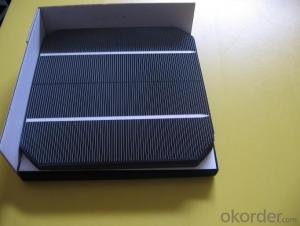
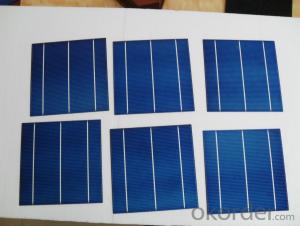
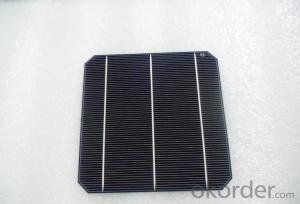
3BB Monocrystallin Best Solar Cell Price
1.Size: 6*6 solar cell
2. Efficiency:4.3WMonocrystallin Best Solar Cell Price
6 Inch 3BB Monocrystallin Best Solar Cell Price
Dimension: 156mm x 156mm
Diagonal: 200mm (round chamfers)
Front: Anisotropically texturized surface and dark silicon nitride
anti-reflection coating
1.9mm silver busbars
Back: Full-surface aluminum back-surface field
4.0mm (silver / aluminum) continuous soldering pads
Features
1.High conversion efficiencies resulting in superior power output performance.
2.Outstanding power output even in low light or high temperature conditions
3.Optimized design for ease of soldering and lamination
4.Long-term stability,reliability and performance
5.Low breakage rate
6.Color uniformaity
Packaging & Shipping
1. Item are only shipped after PAYMENT is received.
2.Originally our solar cells are 100 pieces per box, 10 boxes per carton.
2. Please check out your ADDRESS carefully when processing order.
3. Please CONTACT us ASAP if you haven't received the parcel.
Shipping will be made via EMS, DHL, Fedex, UPS , TNT etc
FAQ:
FAQ:
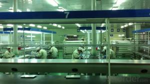
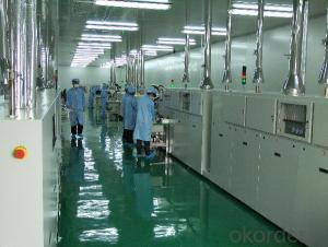
1. Q: Do you have your own factory?
A: Yes, we have. Our factory located in Jiangsu
2. Q: How can I visit your factory?
A: Before you visit,please contact us.We will show you the route or arrange a car to pick you up.
3. Q: Do you provide free sample?
A: Commenly we provide paid sample.
4. Q: Could you print our company LOGO on the nameplate and package?
A: Yes, we accept it.And need an Authorization Letter from you.


- Q: What is the role of back contacts on solar silicon wafers?
- The role of back contacts on solar silicon wafers is to provide an electrical connection between the silicon wafer and the external circuitry of the solar cell. They help in collecting the generated electricity from the front surface of the cell and ensure efficient transfer of the electrical current to the external load. Additionally, back contacts also help in providing structural support to the silicon wafer, allowing for easier handling and integration into the overall solar module.
- Q: Can solar silicon wafers be used in solar-powered transportation systems?
- Yes, solar silicon wafers can be used in solar-powered transportation systems. These wafers are commonly used in solar panels to convert sunlight into electricity. In solar-powered transportation systems, solar panels equipped with silicon wafers can be installed on vehicles, such as cars, boats, or drones, to harness solar energy and power their operations. This helps reduce reliance on traditional fuel sources and contributes to a more sustainable and environmentally friendly mode of transportation.
- Q: How many times is the resistance of the same size silicon
- Silicon is one of the largest and most widely used semiconductor materials, and its output and consumption mark the level of a country's electronics industry.
- Q: How is the surface of a solar silicon wafer textured?
- The surface of a solar silicon wafer is textured using various techniques such as chemical etching or mechanical abrasion. These processes create a rough and uneven surface on the wafer, which helps to increase the absorption of sunlight and enhance the efficiency of the solar cell.
- Q: How do solar silicon wafers contribute to reducing air pollution?
- Solar silicon wafers contribute to reducing air pollution by enabling the production of clean energy through solar panels. These wafers are the key component in the manufacturing of solar cells, which convert sunlight into electricity without emitting any harmful gases or pollutants. By harnessing solar power, we can decrease our reliance on fossil fuels and reduce the amount of greenhouse gas emissions released into the atmosphere, thus mitigating air pollution and its associated environmental and health impacts.
- Q: What is a semiconductor silicon device tester
- Then, the image point set circuit is used to realize the isolation of the electrical components and the connecting wires, and the insulation and the insulation of the insulation are not connected with the insulation
- Q: How are solar silicon wafers protected from static electricity damage?
- Solar silicon wafers are protected from static electricity damage through various measures such as grounding the equipment and personnel, using anti-static packaging materials, employing ionization techniques to neutralize static charges, and implementing proper handling procedures to minimize the risk of electrostatic discharge.
- Q: How are solar silicon wafers protected from potential theft?
- Solar silicon wafers are typically protected from potential theft through a combination of security measures. These measures can include physical barriers such as fences, locks, and surveillance cameras to deter unauthorized access. Additionally, solar farms may employ security personnel to monitor the premises and prevent theft. Advanced tracking and monitoring systems can also be installed to detect any suspicious activity and ensure prompt response.
- Q: Can solar silicon wafers be used in aerospace applications?
- Yes, solar silicon wafers can be used in aerospace applications. Solar panels made from silicon wafers are commonly used in satellites and other spacecraft to generate electrical power from sunlight. They are lightweight, durable, and efficient, making them ideal for aerospace applications where power generation is crucial.
- Q: How does surface roughness affect the efficiency of a solar silicon wafer?
- Surface roughness affects the efficiency of a solar silicon wafer by influencing the amount of light that is absorbed and reflected. A smoother surface allows for more light to be absorbed into the wafer, increasing its efficiency. Conversely, a rougher surface scatters and reflects more light, reducing the overall efficiency of the solar cell.
Send your message to us
Ic Grade Solar Silicon Wafer Supplier - 6 inch 3bb Monocrystalline Best Solar Cell Price 17.6%
- Ref Price:
-
- Loading Port:
- Shanghai
- Payment Terms:
- TT OR LC
- Min Order Qty:
- 1000 pc
- Supply Capability:
- 100000 pc/month
OKorder Service Pledge
OKorder Financial Service
Similar products


Hot products


Hot Searches
Related keywords

