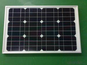


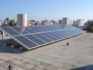

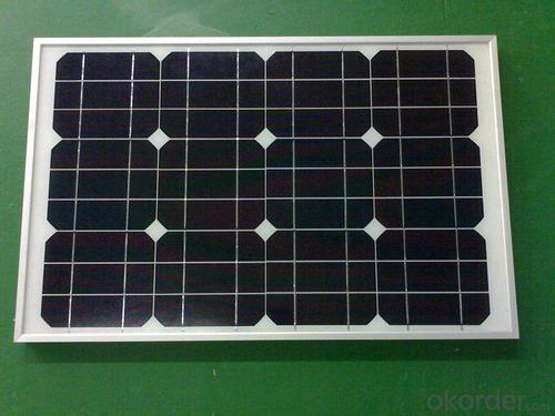
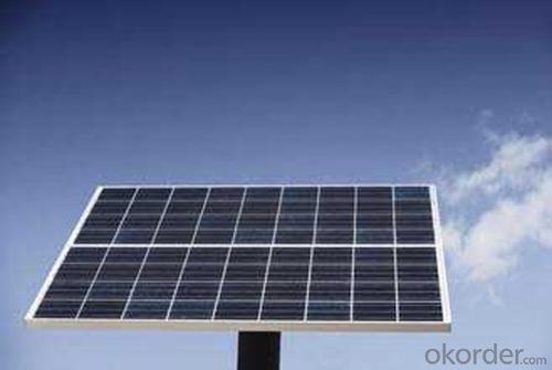

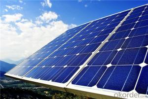
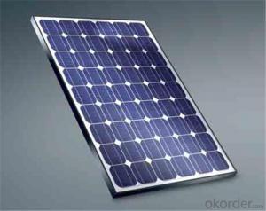
255w Silicone Wafer Solar Panels for Home Use Solar Power System
- Ref Price:
-

- Loading Port:
- China main port
- Payment Terms:
- TT OR LC
- Min Order Qty:
- 10000 watt
- Supply Capability:
- 20000000 watt/month
OKorder Service Pledge
OKorder Financial Service
You Might Also Like


Destription:
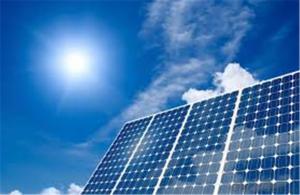
Solar panel refers to a panel designed to absorb the sun's rays as a source of energy for generating electricity or heating. A PV module is a packaged, connected assembly of typically 6×10 solar cells. Solar PV panels constitute the solar array of a photovoltaic system that generates and supplies solar electricity in commercial and residential applications.
Main Characteristic
1.Manufactured according to international quality and Environment Management
System (ISO9001, ISO14001)
2. By the high transmittance, low iron tempered glass, anti-aging of the EVA(polyethylene - vinyl acetate), high-performance crystalline silicon solar cells, good Weather resistance TPT (fluoroplastics composite membrane) by pyramid , has a good Weather resistance and anti-UV, hail, water-proof capacity.
3. OEM and customerized package are accepted
4. High efficiency crystalline silicon solar cells
Quality warranty
1.10 years limited warranty on material and workmanship
2. more than 90% power output in 10 years
3. more than 80% power output in 25 years
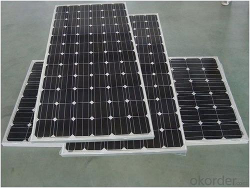
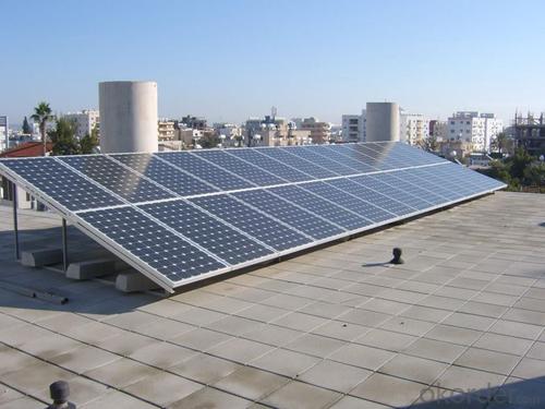
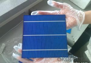
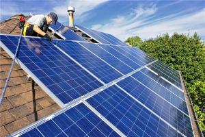
Product show


- Q: Why is it not easy to use high resistance on the silicon chip integrated circuit
- It is not easy to use high resistance on silicon wafer because of the resistance on silicon wafer,
- Q: Can solar silicon wafers be used in hybrid solar cell technologies?
- Yes, solar silicon wafers can be used in hybrid solar cell technologies. Hybrid solar cells combine different materials to enhance efficiency and expand the range of wavelengths they can convert into electricity. Silicon wafers are commonly used in traditional solar cells, and they can also be integrated into hybrid designs, enabling the incorporation of other materials like perovskites or organic semiconductors. This allows for improved performance and increased versatility in capturing solar energy.
- Q: I work in a solar cell company, do silicon chip testing on the human body what chronic harm?
- But if you want to use the laser machine, then pay attention to the laser source.
- Q: How do solar silicon wafers perform in sandy environments?
- Solar silicon wafers perform well in sandy environments as they are designed to be highly durable and resistant to various environmental conditions. The solid construction and protective coatings of the wafers help minimize the negative effects of sand particles, such as scratching or obstructing the surface. However, it is still important to regularly clean the panels to maintain optimal performance and ensure that sand accumulation does not significantly reduce their efficiency.
- Q: How do solar silicon wafers contribute to the electrification of remote areas?
- Solar silicon wafers contribute to the electrification of remote areas by serving as a key component in solar panels. These panels harness the energy from the sun and convert it into electricity, providing a sustainable and reliable power source for off-grid communities. By using solar silicon wafers, remote areas can access clean and renewable energy, reducing their dependence on fossil fuels and improving their living conditions.
- Q: What is the average weight of a solar silicon wafer?
- The average weight of a solar silicon wafer typically ranges from 2 to 4 grams, depending on the size and thickness of the wafer.
- Q: How is the electrical conductivity of a solar silicon wafer measured?
- The electrical conductivity of a solar silicon wafer is typically measured using a four-point probe technique. Four evenly spaced probes are placed on the surface of the wafer, and a known current is passed through the outer probes while the voltage is measured across the inner probes. This method helps eliminate the effects of contact resistance and provides an accurate measurement of the wafer's electrical conductivity.
- Q: Why do you use a concentrated sulfuric acid and hydrogen peroxide to wash silicon?
- But it is best not to use, the use of water under normal conditions and these two kinds of things can be caustic clean silicon, 100% recycled mortar is not the problem, but this requires tens of thousands of cost and appropriate design, I am clean
- Q: Can solar silicon wafers be used in disaster relief efforts?
- Yes, solar silicon wafers can certainly be used in disaster relief efforts. They can be utilized to quickly set up temporary or portable solar power systems, providing electricity for emergency communication devices, lighting, medical equipment, and other essential needs in disaster-affected areas where traditional power sources may be disrupted or unavailable. The versatility and efficiency of solar silicon wafers make them a valuable resource in helping communities during times of crisis and aiding in the recovery process.
- Q: What are the main factors that affect the cost of a solar silicon wafer?
- The main factors that affect the cost of a solar silicon wafer include the raw material costs, manufacturing processes, economies of scale, technological advancements, and market demand.
Send your message to us
255w Silicone Wafer Solar Panels for Home Use Solar Power System
- Ref Price:
-
- Loading Port:
- China main port
- Payment Terms:
- TT OR LC
- Min Order Qty:
- 10000 watt
- Supply Capability:
- 20000000 watt/month
OKorder Service Pledge
OKorder Financial Service
Similar products

Hot products


Hot Searches
Related keywords

