


China Solar Silicon Wafer Cassette - High Quality A Grade Polycrystalline Solar Cell 5V 15.8%
- Ref Price:
-

- Loading Port:
- Shanghai
- Payment Terms:
- TT OR LC
- Min Order Qty:
- 1000 pc
- Supply Capability:
- 100000 pc/month
OKorder Service Pledge
OKorder Financial Service
You Might Also Like


Specifications
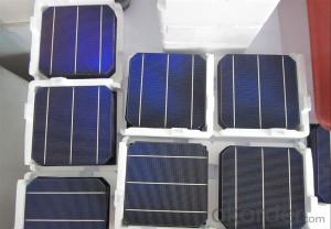
hot sale solar cell
1.16.8%~18.25% high efficiency
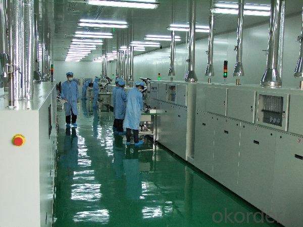
2.100% checked quality
3.ISO9001/ISO14001/TUV/CE/UL
4.stable performance
We can offer you the best quality products and services, don't miss !
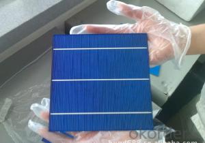
POLY6'(156*156)
Polycrystalline Silicon Solar cell
Physical Characteristics
Dimension: 156mm×156mm±0.5mm
Diagonal: 220mm±0.5mm
Thickness(Si): 200±20 μm
Front(-) Back(+)
Blue anti-reflecting coating (silicon nitride); Aluminum back surface field;
1.5mm wide bus bars; 2.0mm wide soldering pads;
Distance between bus bars: 51mm . Distance between bus bars :51mm .
Electrical Characteristics
Efficiency(%) | 18.00 | 17.80 | 17.60 | 17.40 | 17.20 | 16.80 | 16.60 | 16.40 | 16.20 | 16.00 | 15.80 | 15.60 |
Pmpp(W) | 4.33 | 4.29 | 4.24 | 4.19 | 4.14 | 4.09 | 4.04 | 3.99 | 3.94 | 3.90 | 3.86 | 3.82 |
Umpp(V) | 0.530 | 0.527 | 0.524 | 0.521 | 0.518 | 0.516 | 0.514 | 0.511 | 0.509 | 0.506 | 0.503 | 0.501 |
Impp(A) | 8.159 | 8.126 | 8.081 | 8.035 | 7.990 | 7.938 | 7.876 | 7.813 | 7.754 | 7.698 | 7.642 | 7.586 |
Uoc(V) | 0.633 | 0.631 | 0.628 | 0.625 | 0.623 | 0.620 | 0.618 | 0.617 | 0.615 | 0.613 | 0.611 | 0.609 |
Isc(A) | 8.709 | 8.677 | 8.629 | 8.578 | 8.531 | 8.478 | 8.419 | 8.356 | 8.289 | 8.220 | 8.151 | 8.083 |

MONO5'(125*125mm)165
Monocrystalline silicon solar cell
Physical Characteristics
Dimension: 125mm×125mm±0.5mm
Diagonal: 165mm±0.5mm
Thickness(Si): 200±20 μm
Front(-) Back(+)
Blue anti-reflecting coating(silicon nitride); Aluminum back surface field;
1.6mmwide bus bars; 2.5mm wide soldering pads;
Distance between bus bars: 61mm . Distance between bus bars :61mm .
Electrical Characteristics
Efficiency(%) | 19.40 | 19.20 | 19.00 | 18.80 | 18.60 | 18.40 | 18.20 | 18.00 | 17.80 | 17.60 | 17.40 | 17.20 |
Pmpp(W) | 2.97 | 2.94 | 2.91 | 2.88 | 2.85 | 2.82 | 2.79 | 2.76 | 2.73 | 2.70 | 2.67 | 2.62 |
Umpp(V) | 0.537 | 0.535 | 0.533 | 0.531 | 0.527 | 0.524 | 0.521 | 0.518 | 0.516 | 0.515 | 0.513 | 0.509 |
Impp(A) | 5.531 | 5.495 | 5.460 | 5.424 | 5.408 | 5.382 | 5.355 | 5.328 | 5.291 | 5.243 | 5.195 | 4.147 |
Uoc(V) | 0.637 | 0.637 | 0.636 | 0.635 | 0.633 | 0.630 | 0.629 | 0.629 | 0.628 | 0.626 | 0.626 | 0.625 |
Isc(A) | 5.888 | 5.876 | 5.862 | 5.848 | 5.839 | 5.826 | 5.809 | 5.791 | 5.779 | 5.756 | 5.293 | 5.144 |

FAQ:
Q:How can i get some sample?
A:Yes , if you want order ,sample is not a problem.
Q:How about your solar panel efficency?
A: Our product efficency around 17.25%~18.25%.
Q:What’s the certificate you have got?
A: we have overall product certificate of ISO9001/ISO14001/CE/TUV/UL
- Q: Are solar silicon wafers affected by electromagnetic interference (EMI)?
- Yes, solar silicon wafers can be affected by electromagnetic interference (EMI). EMI can disrupt the electrical performance of solar cells, leading to reduced efficiency and output. Therefore, it is important to design solar installations with proper EMI mitigation measures in place to minimize any potential negative impacts.
- Q: Can solar silicon wafers be used in solar-powered space vehicles?
- Yes, solar silicon wafers can be used in solar-powered space vehicles. Solar silicon wafers are commonly used in photovoltaic systems to convert sunlight into electricity. In space, where there is abundant sunlight, solar panels made with silicon wafers can efficiently capture and convert solar energy into electrical power to operate various systems and equipment onboard the space vehicles.
- Q: What is the current industry standard for solar silicon wafer thickness?
- The current industry standard for solar silicon wafer thickness is typically around 180 to 200 micrometers (μm).
- Q: What is the typical size of a solar silicon wafer?
- The typical size of a solar silicon wafer is around 156mm or 6 inches in diameter.
- Q: What are the different types of anti-reflective coatings used on solar silicon wafers?
- There are primarily two types of anti-reflective coatings used on solar silicon wafers: silicon nitride (SiN) and titanium dioxide (TiO2) coatings. These coatings help reduce the reflection of sunlight, thereby increasing the efficiency of solar cells by allowing more light to be absorbed.
- Q: Are there any limitations to the size of solar silicon wafers that can be produced?
- Yes, there are limitations to the size of solar silicon wafers that can be produced. Currently, the industry standard for solar panels is based on silicon wafers that are typically 156mm x 156mm or 210mm x 210mm in size. These dimensions are determined by several factors, including the manufacturing process, material properties, and handling constraints. While larger wafers may offer advantages in terms of increased efficiency and reduced costs, their production and handling become more challenging. Additionally, the size of the wafers is also constrained by the size of the equipment used in solar panel manufacturing. However, ongoing research and technological advancements may lead to further increases in the size of solar silicon wafers in the future.
- Q: What are the main manufacturers of solar silicon wafers?
- Some of the main manufacturers of solar silicon wafers include companies like REC Silicon, Wacker Chemie, Hemlock Semiconductor Corporation, and Shin-Etsu Chemical Co., Ltd.
- Q: What is the role of back surface field in solar silicon wafers?
- The role of the back surface field in solar silicon wafers is to enhance the efficiency of the solar cell by reducing recombination and increasing the collection of charge carriers generated by sunlight. It creates a strong electric field at the back surface of the wafer, pushing the minority carriers towards the front surface, where they can be collected and harnessed to generate electricity.
- Q: What are the main challenges in the production of solar silicon wafers?
- One of the main challenges in the production of solar silicon wafers is the high energy consumption involved in the manufacturing process. The production of silicon wafers requires a significant amount of energy, particularly during the purification and crystallization stages. This poses a challenge in terms of the environmental impact and the overall sustainability of the process. Another challenge is the high cost associated with producing high-quality silicon wafers. The fabrication process requires precise control over various parameters such as temperature, pressure, and impurity levels, which can be expensive to maintain. Additionally, the raw materials used in the production, such as high-purity silicon, are costly, further adding to the overall production expenses. Furthermore, ensuring consistent and uniform quality across all produced wafers is another challenge. Variations in thickness, impurity levels, and crystal structure can have a significant impact on the efficiency and performance of solar cells. Thus, maintaining strict quality control measures throughout the production process is crucial but can be technically demanding and time-consuming. Lastly, the production of silicon wafers also generates a considerable amount of waste, including silicon dust and other byproducts. Proper disposal and recycling of these waste materials pose a challenge in terms of environmental sustainability and efficient resource management. Overall, addressing these challenges in energy consumption, cost, quality control, and waste management is essential to enhance the efficiency and sustainability of solar silicon wafer production.
- Q: How does the efficiency of a solar silicon wafer change with time of day?
- The efficiency of a solar silicon wafer typically fluctuates with the time of day. It tends to be highest during peak sunlight hours, which are typically around midday, and decreases as the sun moves closer to sunrise or sunset. This is because the intensity of sunlight is strongest when the sun is directly overhead, providing maximum energy for the solar panel to convert into electricity. As the angle of the sun changes throughout the day, the amount of sunlight reaching the solar wafer reduces, resulting in a decrease in efficiency.
Send your message to us
China Solar Silicon Wafer Cassette - High Quality A Grade Polycrystalline Solar Cell 5V 15.8%
- Ref Price:
-
- Loading Port:
- Shanghai
- Payment Terms:
- TT OR LC
- Min Order Qty:
- 1000 pc
- Supply Capability:
- 100000 pc/month
OKorder Service Pledge
OKorder Financial Service
Similar products


Hot products


Hot Searches
Related keywords

