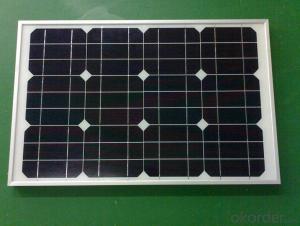

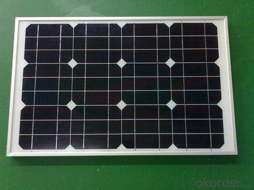

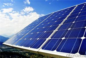
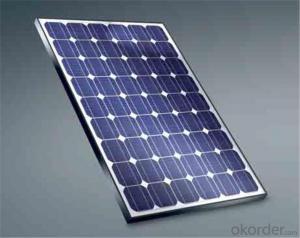
250W Solar Silicon Wafer Panels for Home Use Solar Power System
- Ref Price:
-

- Loading Port:
- China main port
- Payment Terms:
- TT OR LC
- Min Order Qty:
- 10000 watt
- Supply Capability:
- 20000000 watt/month
OKorder Service Pledge
OKorder Financial Service
You Might Also Like


Destription:
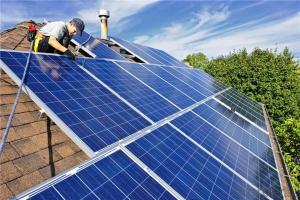
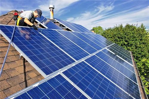
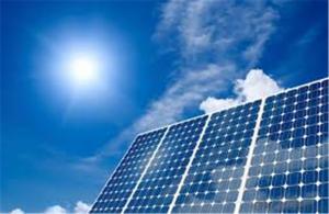
Solar panel refers to a panel designed to absorb the sun's rays as a source of energy for generating electricity or heating. A PV module is a packaged, connected assembly of typically 6×10 solar cells. Solar PV panels constitute the solar array of a photovoltaic system that generates and supplies solar electricity in commercial and residential applications.
Main Characteristic
1.Manufactured according to international quality and Environment Management
System (ISO9001, ISO14001)
2. By the high transmittance, low iron tempered glass, anti-aging of the EVA(polyethylene - vinyl acetate), high-performance crystalline silicon solar cells, good Weather resistance TPT (fluoroplastics composite membrane) by pyramid , has a good Weather resistance and anti-UV, hail, water-proof capacity.
3. OEM and customerized package are accepted
4. High efficiency crystalline silicon solar cells
Quality warranty
1.10 years limited warranty on material and workmanship
2. more than 90% power output in 10 years
3. more than 80% power output in 25 years
Product show


- Q: In the silicon surface cleaning, there is a final step, the silicon chip into the 4% concentration of HF solution soak for five minutes, to hydrogen passivation treatment, and then rinse with deionized water after nitrogen drying,What is the role and mechanism of this hydrogen passivation?
- When the concentration of NaOH is higher than 20%W/V, the corrosion rate depends mainly on the temperature of the solution, but not on the actual concentration of the alkali solution.Removal of surface oxide layer on silicon wafer by HF:
- Q: How do solar silicon wafers contribute to reducing the risk of power outages?
- Solar silicon wafers, which are the key component in solar panels, contribute to reducing the risk of power outages by harnessing solar energy and converting it into electricity. This renewable energy source helps diversify the power generation mix, reducing reliance on fossil fuels and decreasing the strain on the power grid. As solar panels generate electricity during the daytime, when demand is typically high, they help meet peak load requirements and prevent overloading or blackouts. By providing a decentralized and distributed energy source, solar silicon wafers enhance the resilience and reliability of the power system, mitigating the risk of power outages.
- Q: What is the role of the front contact on a solar silicon wafer?
- The role of the front contact on a solar silicon wafer is to collect and transport the generated electricity from the sunlight absorbed by the solar cells. It acts as a conducting layer that allows the flow of electrons, enabling the conversion of solar energy into usable electrical energy. Additionally, the front contact also helps to protect the underlying layers of the solar cell from external elements and provides structural support to the wafer.
- Q: How is the purity of silicon determined for solar wafers?
- The purity of silicon for solar wafers is determined through various analytical techniques such as mass spectrometry, spectroscopy, and resistivity measurement. These methods help identify and quantify impurities like metals, oxygen, carbon, and other elements that may affect the efficiency and performance of the solar cells. Additionally, advanced purification processes are employed to ensure the highest level of purity, resulting in highly efficient solar wafers for photovoltaic applications.
- Q: How do solar silicon wafers perform in high-wind conditions?
- Solar silicon wafers are generally designed to withstand high-wind conditions. They are made from sturdy materials and undergo rigorous testing to ensure durability. Additionally, solar panels are typically mounted securely onto structures to minimize the impact of strong winds. While extremely powerful winds may cause some stress on the panels, proper installation and design measures help to ensure their performance and longevity even in high-wind conditions.
- Q: How are solar silicon wafers protected from chemical damage during manufacturing?
- Solar silicon wafers are protected from chemical damage during manufacturing through various methods. One common technique involves using a thin layer of passivation material, such as silicon nitride or silicon dioxide, to create a protective coating on the surface of the wafer. This coating acts as a barrier, preventing direct contact between the wafer and potentially harmful chemicals. Additionally, proper handling and storage protocols are followed to minimize exposure to chemicals that could cause damage.
- Q: Can solar silicon wafers be used in other electronic devices?
- Yes, solar silicon wafers can be used in other electronic devices. While their primary use is in solar panels to convert sunlight into electricity, they can also be utilized in various electronic applications such as semiconductors, integrated circuits, and sensors.
- Q: How do solar silicon wafers handle extreme temperatures?
- Solar silicon wafers are designed to handle extreme temperatures quite well. They typically have a high melting point and can withstand temperatures ranging from extremely cold to very hot without significant damage. This is due to the high purity and crystalline structure of the silicon material used in their construction. Additionally, solar panels are often equipped with thermal management systems to dissipate excess heat and prevent any adverse effects on the wafers. Overall, solar silicon wafers are engineered to endure extreme temperature conditions and maintain their efficiency and reliability in various climates.
- Q: Can solar silicon wafers be used in solar-powered cell towers?
- Yes, solar silicon wafers can be used in solar-powered cell towers. These wafers are an essential component of solar panels, which convert sunlight into electricity. Solar panels can be installed on cell towers to harness solar energy and power the tower's equipment, reducing reliance on traditional grid electricity.
- Q: How is the demand for solar silicon wafers expected to grow in the future?
- The demand for solar silicon wafers is expected to grow significantly in the future due to the increasing adoption of solar energy as a sustainable and renewable source of power. As countries and industries shift towards clean energy solutions, the demand for solar panels, which heavily rely on silicon wafers, is projected to rise. Additionally, advancements in technology and manufacturing processes are likely to drive down costs, making solar power more accessible and further boosting the demand for silicon wafers.
Send your message to us
250W Solar Silicon Wafer Panels for Home Use Solar Power System
- Ref Price:
-
- Loading Port:
- China main port
- Payment Terms:
- TT OR LC
- Min Order Qty:
- 10000 watt
- Supply Capability:
- 20000000 watt/month
OKorder Service Pledge
OKorder Financial Service
Similar products

Hot products


Hot Searches
Related keywords

