


Solar Silicon Wafer for Sale - High Quality A Grade Monocrystalline 5V 19.2% Solar Cell
- Ref Price:
-

- Loading Port:
- Shanghai
- Payment Terms:
- TT OR LC
- Min Order Qty:
- 1000 pc
- Supply Capability:
- 100000 pc/month
OKorder Service Pledge
OKorder Financial Service
You Might Also Like


Specifications
hot sale solar cell
1.16.8%~18.25% high efficiency
2.100% checked quality
3.ISO9001/ISO14001/TUV/CE/UL
4.stable performance
We can offer you the best quality products and services, don't miss !
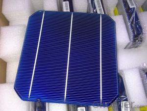
POLY6'(156*156)
Polycrystalline Silicon Solar cell
Physical Characteristics
Dimension: 156mm×156mm±0.5mm
Diagonal: 220mm±0.5mm
Thickness(Si): 200±20 μm
Front(-) Back(+)
Blue anti-reflecting coating (silicon nitride); Aluminum back surface field;
1.5mm wide bus bars; 2.0mm wide soldering pads;
Distance between bus bars: 51mm . Distance between bus bars :51mm .
Electrical Characteristics
Efficiency(%) | 18.00 | 17.80 | 17.60 | 17.40 | 17.20 | 16.80 | 16.60 | 16.40 | 16.20 | 16.00 | 15.80 | 15.60 |
Pmpp(W) | 4.33 | 4.29 | 4.24 | 4.19 | 4.14 | 4.09 | 4.04 | 3.99 | 3.94 | 3.90 | 3.86 | 3.82 |
Umpp(V) | 0.530 | 0.527 | 0.524 | 0.521 | 0.518 | 0.516 | 0.514 | 0.511 | 0.509 | 0.506 | 0.503 | 0.501 |
Impp(A) | 8.159 | 8.126 | 8.081 | 8.035 | 7.990 | 7.938 | 7.876 | 7.813 | 7.754 | 7.698 | 7.642 | 7.586 |
Uoc(V) | 0.633 | 0.631 | 0.628 | 0.625 | 0.623 | 0.620 | 0.618 | 0.617 | 0.615 | 0.613 | 0.611 | 0.609 |
Isc(A) | 8.709 | 8.677 | 8.629 | 8.578 | 8.531 | 8.478 | 8.419 | 8.356 | 8.289 | 8.220 | 8.151 | 8.083 |

MONO5'(125*125mm)165
Monocrystalline silicon solar cell
Physical Characteristics
Dimension: 125mm×125mm±0.5mm
Diagonal: 165mm±0.5mm
Thickness(Si): 200±20 μm
Front(-) Back(+)
Blue anti-reflecting coating(silicon nitride); Aluminum back surface field;
1.6mmwide bus bars; 2.5mm wide soldering pads;
Distance between bus bars: 61mm . Distance between bus bars :61mm .
Electrical Characteristics
Efficiency(%) | 19.40 | 19.20 | 19.00 | 18.80 | 18.60 | 18.40 | 18.20 | 18.00 | 17.80 | 17.60 | 17.40 | 17.20 |
Pmpp(W) | 2.97 | 2.94 | 2.91 | 2.88 | 2.85 | 2.82 | 2.79 | 2.76 | 2.73 | 2.70 | 2.67 | 2.62 |
Umpp(V) | 0.537 | 0.535 | 0.533 | 0.531 | 0.527 | 0.524 | 0.521 | 0.518 | 0.516 | 0.515 | 0.513 | 0.509 |
Impp(A) | 5.531 | 5.495 | 5.460 | 5.424 | 5.408 | 5.382 | 5.355 | 5.328 | 5.291 | 5.243 | 5.195 | 4.147 |
Uoc(V) | 0.637 | 0.637 | 0.636 | 0.635 | 0.633 | 0.630 | 0.629 | 0.629 | 0.628 | 0.626 | 0.626 | 0.625 |
Isc(A) | 5.888 | 5.876 | 5.862 | 5.848 | 5.839 | 5.826 | 5.809 | 5.791 | 5.779 | 5.756 | 5.293 | 5.144 |

FAQ:
Q:How can i get some sample?
A:Yes , if you want order ,sample is not a problem.
Q:How about your solar panel efficency?
A: Our product efficency around 17.25%~18.25%.
Q:What’s the certificate you have got?
A: we have overall product certificate of ISO9001/ISO14001/CE/TUV/UL
- Q: What is the role of a frame in a solar silicon wafer?
- The role of a frame in a solar silicon wafer is to provide support and protection to the wafer during the manufacturing process and throughout its lifespan. It helps maintain the structural integrity of the wafer, preventing it from warping or breaking. Additionally, the frame allows for easy handling, transportation, and installation of the wafer in solar panels.
- Q: In the silicon surface cleaning, there is a final step, the silicon chip into the 4% concentration of HF solution soak for five minutes, to hydrogen passivation treatment, and then rinse with deionized water after nitrogen drying,What is the role and mechanism of this hydrogen passivation?
- 0.5 ~ 1min in order to achieve the effect of removing the damage layer, at this timeCorrosion rate can reach 6 to 10um/min.In the polishing process to remove the damage layer on the basis to try to reduce, to prevent corrosion of the wafer was too thin.
- Q: How are solar silicon wafers protected from electrical faults or short circuits?
- Solar silicon wafers are protected from electrical faults or short circuits through various methods, such as the implementation of anti-reflective coatings, passivation layers, and junction boxes. These protective measures help to prevent direct contact between the conducting materials and the silicon wafer, reducing the likelihood of electrical faults or short circuits. Additionally, quality control measures during the manufacturing process ensure that the wafers are free from any defects or impurities that could potentially lead to electrical issues.
- Q: How many times is the resistance of the same size silicon
- Silicon is an important semiconductor material, chemical element symbol Si, the silicon used in the electronic industry should have high purity and excellent electrical and mechanical properties
- Q: How do solar silicon wafers perform in earthquake-prone environments?
- Solar silicon wafers perform well in earthquake-prone environments due to their inherent durability and flexibility. The rigid structure of the wafers allows them to withstand seismic activities without significant damage or loss of functionality. Additionally, advancements in solar panel mounting systems have further enhanced their resilience by incorporating features such as shock-absorbing mechanisms and reinforced support structures. Overall, solar silicon wafers have proven to be reliable and robust in earthquake-prone areas, ensuring the continuous generation of clean energy.
- Q: What is the cost of a solar silicon wafer?
- The cost of a solar silicon wafer can vary depending on various factors such as size, quality, and market conditions. On average, the cost of a standard silicon wafer used in solar panels ranges from $0.10 to $0.30 per watt. However, it is important to note that prices may fluctuate due to factors like supply and demand, technological advancements, and economies of scale.
- Q: How do solar silicon wafers contribute to reducing greenhouse gas emissions?
- Solar silicon wafers contribute to reducing greenhouse gas emissions by enabling the production of solar panels, which generate clean and renewable electricity. As silicon wafers are the key component of photovoltaic cells, they absorb sunlight and convert it into usable energy, eliminating the need for fossil fuel-based power generation. By replacing traditional energy sources with solar power, greenhouse gas emissions from power plants and other fossil fuel combustion processes are significantly reduced, consequently mitigating climate change and promoting a more sustainable future.
- Q: Can solar silicon wafers be used in thin-film solar cell technology?
- No, solar silicon wafers cannot be used in thin-film solar cell technology. Thin-film solar cells are typically made of materials like amorphous silicon, cadmium telluride, or copper indium gallium selenide, which are deposited as thin layers onto a substrate, eliminating the need for silicon wafers.
- Q: Can solar silicon wafers be used in marine or offshore applications?
- Yes, solar silicon wafers can be used in marine or offshore applications. However, special considerations need to be taken into account due to the harsh marine environment, such as protection against corrosion, water resistance, and durability against high winds and saltwater exposure.
- Q: What is the composition of a solar silicon wafer?
- A solar silicon wafer is primarily composed of high-purity crystalline silicon.
Send your message to us
Solar Silicon Wafer for Sale - High Quality A Grade Monocrystalline 5V 19.2% Solar Cell
- Ref Price:
-
- Loading Port:
- Shanghai
- Payment Terms:
- TT OR LC
- Min Order Qty:
- 1000 pc
- Supply Capability:
- 100000 pc/month
OKorder Service Pledge
OKorder Financial Service
Similar products


Hot products


Hot Searches
Related keywords

