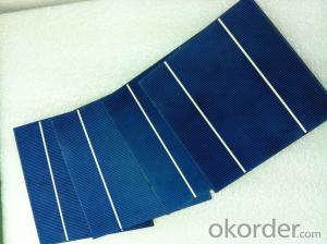
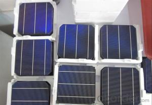
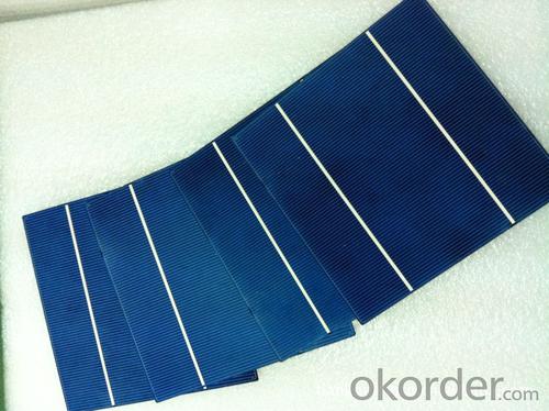


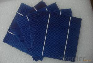
Solar Silicon Wafer Cassette Compatible High Current 17.2% Polycrystalline Silicon Solar Cell
- Ref Price:
-

- Loading Port:
- Shanghai
- Payment Terms:
- TT OR LC
- Min Order Qty:
- 1000 pc
- Supply Capability:
- 100000 pc/month
OKorder Service Pledge
OKorder Financial Service
You Might Also Like


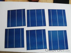
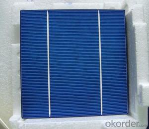
4 Bus Bars 156*156 17.6% efficiency poly solar cell
PHYSICAL CHARACTERISTICS
Dimension: 156mm x 156mm ± 0.5mm
Wafer Thickeness: 180um+20um and 200um+20um
Front(-) Four 1.2mm silver busbar
Silicon nitride blue anti-reflection coating
Back(+) aluminum back surface field
1.75mm(silver) wide segment soldering pads

Typical Electrical Characteristics
Efficiency | W(Pmpp) | V(Umpp) | A(Impp) | V(Uoc) | A(Isc) |
17.4-17.5 | 4.234 | 0.517 | 8.231 | 0.622 | 8.759 |
17.5-17.6 | 4.259 | 0.519 | 8.243 | 0.623 | 8.769 |
17.7-17.8 | 4.283 | 0.521 | 8.256 | 0.625 | 8.779 |
17.8-17.9 | 4.307 | 0.523 | 8.268 | 0.626 | 8.788 |
17.9-18.0 | 4.332 | 0.525 | 8.281 | 0.627 | 8.798 |
18.0-18.1 | 4.380 | 0.529 | 8.306 | 0.629 | 8.808 |
18.1-18.2 | 4.405 | 0.531 | 8.318 | 0.632 | 8.818 |
18.2-18.3 | 4.429 | 0.533 | 8.331 | 0.633 | 8.837 |
18.3-18.4 | 4.453 | 0.535 | 8.344 | 0.634 | 8.847 |
18.4-18.5 | 4.478 | 0.537 | 8.356 | 0.636 | 8.856 |
18.5-18.6 | 4.502 | 0.539 | 8.369 | 0.637 | 8.866 |
Efficiency | W(Pmpp) | V(Umpp) | A(Impp) | V(Uoc) | A(Isc) |
20.90-21.00 | 5.06 | 0.557 | 9.007 | 0.653 | 9.688 |
20.80-20.90 | 5.04 | 0.556 | 9.062 | 0.652 | 9.683 |
20.70-20.80 | 5.02 | 0.554 | 9.055 | 0.651 | 9.684 |
20.60-20.70 | 4.99 | 0.552 | 9.033 | 0.651 | 9.672 |
20.50-20.60 | 4.97 | 0.550 | 9.002 | 0.650 | 9.673 |
20.40-20.50 | 4.94 | 0.548 | 9.012 | 0.649 | 9.674 |
20.30-20.40 | 4.92 | 0.546 | 9.009 | 0.649 | 9.655 |
20.20-20.30 | 4.89 | 0.543 | 9.012 | 0.648 | 9.634 |
20.10-20.20 | 4.87 | 0.541 | 8.998 | 0.648 | 9.617 |
20.00-20.10 | 4.85 | 0.540 | 8.977 | 0.647 | 9.600 |
*Data under standard testing conditional (STC):1,000w/m2,AM1.5, 25°C , Pmax:Positive power tolerance.
3 Bus Bars 156*156 17.4% efficiency poly solar cell
Dimension: 156 mm x 156 mm ± 0.5 mm
Wafer Thickeness: 156 mm x 156 mm ± 0.5 mm

Typical Electrical Characteristics:
| Efficiency code | 1660 | 1680 | 1700 | 1720 | 1740 | 1760 | 1780 | 1800 | 1820 | 1840 | 1860 |
| Efficiency (%) | 16.6 | 16.8 | 17.0 | 17.2 | 17.4 | 17.6 | 17.8 | 18.0 | 18.2 | 18.4 | 18.6 |
| Pmax (W) | 4.04 | 4.09 | 4.14 | 4.19 | 4.23 | 4.28 | 4.33 | 4.38 | 4.43 | 4.48 | 4.53 |
| Voc (V) | 0.612 | 0.615 | 0.618 | 0.621 | 0.624 | 0.627 | 0.629 | 0.63 | 0.633 | 0.635 | 0.637 |
| Isc (A) | 8.42 | 8.46 | 8.51 | 8.56 | 8.61 | 8.65 | 8.69 | 8.73 | 8.77 | 8.81 | 8.84 |
| Imp (A) | 7.91 | 7.99 | 8.08 | 8.16 | 8.22 | 8.27 | 8.33 | 8.38 | 8.43 | 8.48 | 8.53 |
* Testing conditions: 1000 W/m2, AM 1.5, 25 °C, Tolerance: Efficiency ± 0.2% abs., Pmpp ±1.5% rel.
* Imin : at 0.5 V
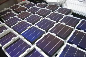
Production:

Package:

FAQ:
1. Q: Do you have your own factory?
A: Yes, we have. Our factory located in Jiangsu
2. Q: How can I visit your factory?
A: Before you visit,please contact us.We will show you the route or arrange a car to pick you up.
3. Q: Do you provide free sample?
A: Commenly we provide paid sample.
4. Q: Could you print our company LOGO on the nameplate and package?
A: Yes, we accept it.And need an Authorization Letter from you.
5. Q: Do you accept custom design on size?
A: Yes, if the size is reasonable.
6. Q: How can I be your agent in my country?
A: Please leave feedback. It's better for us to talk about details by email.
7. Q: Do you have solar project engineer who can guide me to install system?
A: Yes, we have a professional engineer team. They can teach you how to install a solar system.
- Q: How are solar silicon wafers tested for quality control?
- Solar silicon wafers are tested for quality control through various methods. These include visual inspection to identify any defects or impurities on the surface, measurement of electrical properties such as resistivity and efficiency, and testing for mechanical strength and durability. Additionally, the wafers may undergo spectroscopic analysis to determine their chemical composition and purity. These comprehensive testing procedures ensure that only high-quality silicon wafers meet the required standards for solar panel production.
- Q: Such as the title, look at some of the information, said the integrated circuit are integrated in silicon, why? Why not integrate on insulator?
- First of all, the general circuit of the insulator, just a carrier, it plays the role of support and insulation. As for the integrated circuit, the bottom layer is called the substrate (generally P type semiconductor), is to participate in the work of integrated circuits. CMOS process, so the Nmos substrate are connected together, are the same substrate.
- Q: How do solar silicon wafers contribute to the overall cost of a solar panel?
- Solar silicon wafers are a significant contributor to the overall cost of a solar panel. They account for a substantial portion of the manufacturing expenses due to the high cost of raw materials and the complex fabrication process involved. The efficiency and quality of these wafers directly impact the efficiency and durability of the solar panel, making them an essential component. Therefore, the cost of solar silicon wafers plays a crucial role in determining the final price of a solar panel.
- Q: How are solar silicon wafers connected in a solar array?
- Solar silicon wafers are typically connected in a solar array using soldering or conductive adhesive materials. The wafers are electrically interconnected by soldering or attaching metal ribbons or busbars to their contacts, creating a series of parallel connections. This series of interconnected wafers forms a solar cell module, which is then further connected to other modules to create a larger solar array.
- Q: What are the different materials used for passivation layers in solar silicon wafers?
- The different materials used for passivation layers in solar silicon wafers include silicon nitride (SiNx), aluminum oxide (Al2O3), and silicon oxide (SiO2). These materials are applied as thin films on the surface of the wafers to enhance their energy conversion efficiency and protect them from external factors such as moisture and contamination.
- Q: What are the main differences between monocrystalline and polycrystalline solar silicon wafers?
- The main differences between monocrystalline and polycrystalline solar silicon wafers lie in their fabrication process and efficiency. Monocrystalline wafers are made from a single crystal structure, resulting in a uniform and pure composition. This allows them to have higher efficiency and power output, making them more suitable for applications with limited space. On the other hand, polycrystalline wafers are made from multiple crystal structures, which leads to lower efficiency and slightly lower power output. However, they are less expensive to produce and can still be effective in larger installations where space is not a constraint.
- Q: Are there any environmental concerns associated with solar silicon wafers?
- Yes, there are some environmental concerns associated with solar silicon wafers. The primary concern is the energy-intensive manufacturing process of silicon wafers, which requires a significant amount of electricity and raw materials. The production of silicon wafers also generates hazardous waste, including toxic chemicals and greenhouse gas emissions. Additionally, the mining of raw materials like quartz and silicon for the production of wafers can have negative environmental impacts, such as habitat destruction and water pollution. However, it is important to note that compared to other forms of energy generation, solar silicon wafers have relatively minimal environmental impacts over their lifecycle.
- Q: What is the role of surface texturing in solar silicon wafers?
- The role of surface texturing in solar silicon wafers is to enhance light trapping and increase the overall efficiency of solar cells. The textured surface helps to reduce reflection and increase the absorption of sunlight, allowing for more effective conversion of solar energy into electricity.
- Q: How are solar silicon wafers protected from humidity and moisture during manufacturing?
- Solar silicon wafers are protected from humidity and moisture during manufacturing through various methods such as encapsulation, hermetic sealing, and the use of protective coatings. These measures help to prevent any potential damage or degradation of the wafers caused by exposure to moisture, ensuring their quality and performance in solar panel production.
- Q: Can solar silicon wafers be used in solar-powered air conditioning systems?
- Yes, solar silicon wafers can be used in solar-powered air conditioning systems. Silicon wafers are commonly used in solar panels to convert sunlight into electricity, which can then be used to power various appliances, including air conditioning systems.
Send your message to us
Solar Silicon Wafer Cassette Compatible High Current 17.2% Polycrystalline Silicon Solar Cell
- Ref Price:
-
- Loading Port:
- Shanghai
- Payment Terms:
- TT OR LC
- Min Order Qty:
- 1000 pc
- Supply Capability:
- 100000 pc/month
OKorder Service Pledge
OKorder Financial Service
Similar products


Hot products


Hot Searches
Related keywords

