


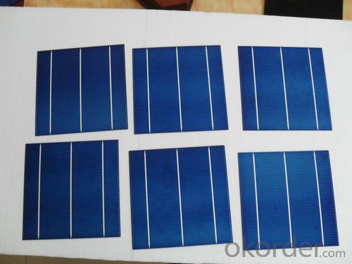


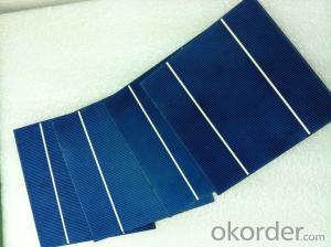
Jinko Solar Silicon Wafer High Current 17.0% Polycrystalline Silicon Solar Cell
- Ref Price:
-

- Loading Port:
- Shanghai
- Payment Terms:
- TT OR LC
- Min Order Qty:
- 1000 pc
- Supply Capability:
- 100000 pc/month
OKorder Service Pledge
OKorder Financial Service
You Might Also Like


4 Bus Bars 156*156 17.6% efficiency poly solar cell
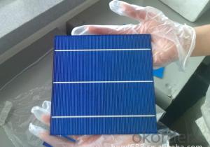
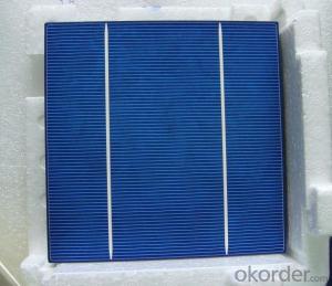
PHYSICAL CHARACTERISTICS
Dimension: 156mm x 156mm ± 0.5mm
Wafer Thickeness: 180um+20um and 200um+20um
Front(-) Four 1.2mm silver busbar
Silicon nitride blue anti-reflection coating
Back(+) aluminum back surface field
1.75mm(silver) wide segment soldering pads

Typical Electrical Characteristics
Efficiency | W(Pmpp) | V(Umpp) | A(Impp) | V(Uoc) | A(Isc) |
17.4-17.5 | 4.234 | 0.517 | 8.231 | 0.622 | 8.759 |
17.5-17.6 | 4.259 | 0.519 | 8.243 | 0.623 | 8.769 |
17.7-17.8 | 4.283 | 0.521 | 8.256 | 0.625 | 8.779 |
17.8-17.9 | 4.307 | 0.523 | 8.268 | 0.626 | 8.788 |
17.9-18.0 | 4.332 | 0.525 | 8.281 | 0.627 | 8.798 |
18.0-18.1 | 4.380 | 0.529 | 8.306 | 0.629 | 8.808 |
18.1-18.2 | 4.405 | 0.531 | 8.318 | 0.632 | 8.818 |
18.2-18.3 | 4.429 | 0.533 | 8.331 | 0.633 | 8.837 |
18.3-18.4 | 4.453 | 0.535 | 8.344 | 0.634 | 8.847 |
18.4-18.5 | 4.478 | 0.537 | 8.356 | 0.636 | 8.856 |
18.5-18.6 | 4.502 | 0.539 | 8.369 | 0.637 | 8.866 |
Efficiency | W(Pmpp) | V(Umpp) | A(Impp) | V(Uoc) | A(Isc) |
20.90-21.00 | 5.06 | 0.557 | 9.007 | 0.653 | 9.688 |
20.80-20.90 | 5.04 | 0.556 | 9.062 | 0.652 | 9.683 |
20.70-20.80 | 5.02 | 0.554 | 9.055 | 0.651 | 9.684 |
20.60-20.70 | 4.99 | 0.552 | 9.033 | 0.651 | 9.672 |
20.50-20.60 | 4.97 | 0.550 | 9.002 | 0.650 | 9.673 |
20.40-20.50 | 4.94 | 0.548 | 9.012 | 0.649 | 9.674 |
20.30-20.40 | 4.92 | 0.546 | 9.009 | 0.649 | 9.655 |
20.20-20.30 | 4.89 | 0.543 | 9.012 | 0.648 | 9.634 |
20.10-20.20 | 4.87 | 0.541 | 8.998 | 0.648 | 9.617 |
20.00-20.10 | 4.85 | 0.540 | 8.977 | 0.647 | 9.600 |
*Data under standard testing conditional (STC):1,000w/m2,AM1.5, 25°C , Pmax:Positive power tolerance.
3 Bus Bars 156*156 17.4% efficiency poly solar cell
Dimension: 156 mm x 156 mm ± 0.5 mm
Wafer Thickeness: 156 mm x 156 mm ± 0.5 mm

Typical Electrical Characteristics:
| Efficiency code | 1660 | 1680 | 1700 | 1720 | 1740 | 1760 | 1780 | 1800 | 1820 | 1840 | 1860 |
| Efficiency (%) | 16.6 | 16.8 | 17.0 | 17.2 | 17.4 | 17.6 | 17.8 | 18.0 | 18.2 | 18.4 | 18.6 |
| Pmax (W) | 4.04 | 4.09 | 4.14 | 4.19 | 4.23 | 4.28 | 4.33 | 4.38 | 4.43 | 4.48 | 4.53 |
| Voc (V) | 0.612 | 0.615 | 0.618 | 0.621 | 0.624 | 0.627 | 0.629 | 0.63 | 0.633 | 0.635 | 0.637 |
| Isc (A) | 8.42 | 8.46 | 8.51 | 8.56 | 8.61 | 8.65 | 8.69 | 8.73 | 8.77 | 8.81 | 8.84 |
| Imp (A) | 7.91 | 7.99 | 8.08 | 8.16 | 8.22 | 8.27 | 8.33 | 8.38 | 8.43 | 8.48 | 8.53 |
* Testing conditions: 1000 W/m2, AM 1.5, 25 °C, Tolerance: Efficiency ± 0.2% abs., Pmpp ±1.5% rel.
* Imin : at 0.5 V
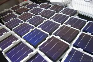
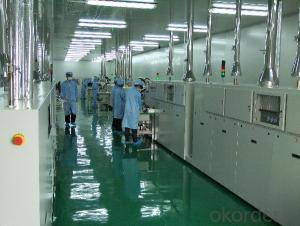
Production:

Package:

FAQ:
1. Q: Do you have your own factory?
A: Yes, we have. Our factory located in Jiangsu
2. Q: How can I visit your factory?
A: Before you visit,please contact us.We will show you the route or arrange a car to pick you up.
3. Q: Do you provide free sample?
A: Commenly we provide paid sample.
4. Q: Could you print our company LOGO on the nameplate and package?
A: Yes, we accept it.And need an Authorization Letter from you.
5. Q: Do you accept custom design on size?
A: Yes, if the size is reasonable.
6. Q: How can I be your agent in my country?
A: Please leave feedback. It's better for us to talk about details by email.
7. Q: Do you have solar project engineer who can guide me to install system?
A: Yes, we have a professional engineer team. They can teach you how to install a solar system.
- Q: Are there any regulations or standards for solar silicon wafers?
- Yes, there are regulations and standards for solar silicon wafers. These regulations and standards are put in place to ensure the quality, efficiency, and safety of solar silicon wafers used in the production of solar cells and panels. They cover various aspects such as the purity of the silicon, thickness and uniformity of the wafer, electrical properties, and environmental sustainability. These regulations and standards are developed and enforced by organizations such as the International Electrotechnical Commission (IEC) and the American Society for Testing and Materials (ASTM). Compliance with these regulations and standards is important for the reliable and effective operation of solar energy systems.
- Q: Can solar silicon wafers be used in remote off-grid locations?
- Yes, solar silicon wafers can be used in remote off-grid locations. Solar panels made from silicon wafers are commonly used to generate electricity in areas without access to a traditional power grid. These panels are designed to capture sunlight and convert it into usable energy, making them suitable for off-grid locations where they can provide a reliable and renewable source of power.
- Q: What is the purpose of a power output in a solar silicon wafer?
- The purpose of a power output in a solar silicon wafer is to convert sunlight into electricity.
- Q: What are the properties of a high-quality solar silicon wafer?
- A high-quality solar silicon wafer possesses several key properties. Firstly, it should have a high level of purity, typically exceeding 99.9999%, to ensure minimal impurities and defects. Additionally, it should exhibit excellent crystallographic orientation and uniformity to enhance the efficiency of solar cells. The wafer's thickness and surface quality are also crucial factors, requiring precise control and minimal imperfections to optimize light absorption and electron movement. Furthermore, a high-quality wafer should have low electrical resistance, allowing efficient charge carrier transport. Lastly, it should possess a low rate of light-induced degradation to ensure long-term stability and performance.
- Q: What is the typical efficiency degradation rate of a solar silicon wafer over time?
- The typical efficiency degradation rate of a solar silicon wafer over time can vary, but it is generally estimated to be around 0.5% to 1% per year.
- Q: What are the different types of glass covers used on solar silicon wafers?
- There are primarily three types of glass covers used on solar silicon wafers: tempered glass, anti-reflective coated glass, and textured glass. Tempered glass provides durability and protection against physical damage. Anti-reflective coated glass minimizes reflection and increases light absorption, enhancing the efficiency of the solar cells. Textured glass has a rough surface, which helps in trapping more sunlight by scattering it within the solar cell.
- Q: Can solar silicon wafers be used in harsh environments?
- Yes, solar silicon wafers can be used in harsh environments. They are designed to withstand various environmental conditions such as extreme temperatures, high humidity, and exposure to UV radiation. The wafers are typically coated with protective materials to enhance their durability and resistance to corrosion, making them suitable for harsh outdoor environments.
- Q: What are the dimensions of a standard solar silicon wafer?
- The dimensions of a standard solar silicon wafer are typically around 156mm in size, with a thickness of around 200 micrometers.
- Q: Can solar silicon wafers be used in all types of solar panels?
- Yes, solar silicon wafers can be used in all types of solar panels. Silicon is the most commonly used material for solar panels, and it can be processed into wafers and used in various types of solar panel technologies such as monocrystalline, polycrystalline, and thin-film.
- Q: Can solar silicon wafers be used in space exploration missions?
- Yes, solar silicon wafers can be used in space exploration missions. Solar panels made from silicon wafers are commonly used to generate electricity in spacecraft and satellites as they can efficiently convert sunlight into electrical energy even in the harsh conditions of space. This sustainable and reliable source of power is crucial for powering various systems and instruments during space missions.
Send your message to us
Jinko Solar Silicon Wafer High Current 17.0% Polycrystalline Silicon Solar Cell
- Ref Price:
-
- Loading Port:
- Shanghai
- Payment Terms:
- TT OR LC
- Min Order Qty:
- 1000 pc
- Supply Capability:
- 100000 pc/month
OKorder Service Pledge
OKorder Financial Service
Similar products

Hot products


Hot Searches
Related keywords

