


Silicon Wafer Solar Cell Panels - Monosolicion Poly 156mm*156mm
- Ref Price:
-

- Loading Port:
- China main port
- Payment Terms:
- TT OR LC
- Min Order Qty:
- 100 watt
- Supply Capability:
- 10000 watt/month
OKorder Service Pledge
Quality Product, Order Online Tracking, Timely Delivery
OKorder Financial Service
Credit Rating, Credit Services, Credit Purchasing
You Might Also Like


Monosolicion Solar Cells Poly 156mm*156mm
Typical electrical characteristics
Efficiency code | 1720 | 1740 | 1760 | 1780 | 1820 | 1840 | |
Efficiency (min) | (%) | 17.2 | 17.4 | 17.6 | 17.8 | 18.2 | 18.4 |
Pmax | (W) | 4.186 | 4.234 | 4.283 | 4.332 | 4.429 | 4.478 |
Voc | (V) | 0.631 | 0.632 | 0.634 | 0.636 | 0.640 | 0.642 |
Isc | (A) | 8.446 | 8.485 | 8.523 | 8.573 | 8.660 | 8.700 |
Vmp | (V) | 0.525 | 0.527 | 0.529 | 0.531 | 0.535 | 0.537 |
Imp | (A) | 7.973 | 8.035 | 8.097 | 8.160 | 8.280 | 8.340 |
Data under standard testing conditions(STC): 1,000W/m2, AM1.5, 25℃, Pmax: Positive power tolerance.
Typical teperature coefficients
Voltage | -2.08 | mV/K |
Current | +4.58 | mA/K |
Power | -0.40 | %/K |
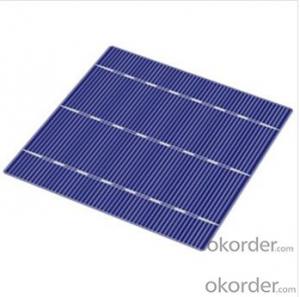
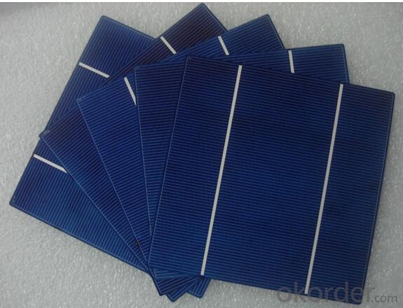
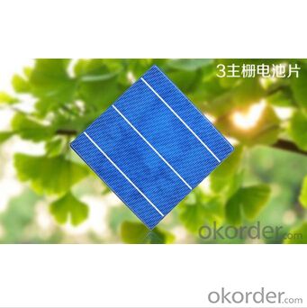
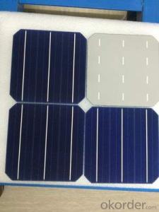
Cell Picture


- Q: How are solar silicon wafers protected from external factors like moisture or dust?
- Solar silicon wafers are typically protected from external factors like moisture or dust through the use of various protective coatings and encapsulation materials. These coatings act as a barrier, preventing any moisture or dust particles from coming into direct contact with the silicon wafer. Additionally, the wafers are often enclosed within a hermetically sealed module, providing further protection against external elements. This combination of coatings and encapsulation helps to ensure the long-term durability and performance of solar silicon wafers in various environmental conditions.
- Q: How are solar silicon wafers protected from environmental factors?
- Solar silicon wafers are protected from environmental factors through a combination of encapsulation and anti-reflective coatings. Encapsulation, typically done with glass or plastic, provides a protective layer that shields the wafer from moisture, dust, and other contaminants. Additionally, anti-reflective coatings are applied to minimize the impact of sunlight reflection, ensuring maximum absorption of solar energy while reducing the risk of damage caused by excessive heat or UV radiation.
- Q: Can solar silicon wafers be used in art installations?
- Yes, solar silicon wafers can be used in art installations. They can serve as a creative medium for artists to incorporate renewable energy elements into their artistic designs.
- Q: Can solar silicon wafers be used in tandem with other types of solar cells?
- Yes, solar silicon wafers can be used in tandem with other types of solar cells. Tandem solar cells, also known as multi-junction solar cells, are devices that consist of multiple layers of different types of solar cells stacked together. By combining solar silicon wafers with other types of solar cells, such as thin-film or perovskite cells, it is possible to achieve higher efficiencies and better performance in converting sunlight into electricity.
- Q: How is an encapsulant applied to a solar silicon wafer?
- An encapsulant is typically applied to a solar silicon wafer by using a process called lamination. In this process, a layer of encapsulant material, usually ethylene-vinyl acetate (EVA), is placed between the silicon wafer and a top layer of glass. The wafer, encapsulant, and glass are then sandwiched together and subjected to heat and pressure. This causes the encapsulant to melt and flow, adhering to the wafer and creating a protective layer that encapsulates the solar cells.
- Q: What is the role of front contacts on solar silicon wafers?
- The role of front contacts on solar silicon wafers is to collect and extract the generated electricity from the solar cells. These contacts are typically made of metal fingers or grids that are placed on the front surface of the solar cell. They enable the flow of current and help in minimizing the resistance and losses, ensuring efficient electricity production from the solar panel.
- Q: What is the thickness of a solar silicon wafer?
- The thickness of a solar silicon wafer typically ranges from 150 to 200 micrometers.
- Q: The significance of silicon wafer heat treatment
- The significance of silicon wafer heat treatmentHeat treatment temperature requirements: 650 + 5 c;The purpose of heat treatment is to restore the true resistivity of Czochralski silicon wafers;
- Q: Are solar silicon wafers affected by voltage fluctuations?
- Yes, solar silicon wafers can be affected by voltage fluctuations. Fluctuations in voltage can impact the performance and efficiency of solar cells, potentially leading to decreased power output. It is important to maintain stable and consistent voltage levels to optimize the performance of solar panels.
- Q: What is the impact of crystal defects on the performance of solar silicon wafers?
- Crystal defects in solar silicon wafers can have a significant impact on their performance. These defects can include impurities, dislocations, and vacancies within the crystal lattice structure. These defects can reduce the efficiency of solar cells by affecting the flow of electrons and the generation of electric current. They can also lead to increased recombination of charge carriers, resulting in decreased power output and overall performance. Therefore, minimizing crystal defects is crucial in order to enhance the efficiency and performance of solar silicon wafers.
Send your message to us
Silicon Wafer Solar Cell Panels - Monosolicion Poly 156mm*156mm
- Ref Price:
-
- Loading Port:
- China main port
- Payment Terms:
- TT OR LC
- Min Order Qty:
- 100 watt
- Supply Capability:
- 10000 watt/month
OKorder Service Pledge
Quality Product, Order Online Tracking, Timely Delivery
OKorder Financial Service
Credit Rating, Credit Services, Credit Purchasing
Similar products


Hot products


Hot Searches
Related keywords

