


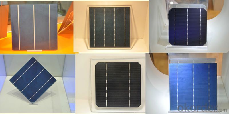


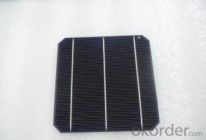
High Quality A Grade Monocrystalline Solar Grade Silicon Wafer Polycrystalline 5v 17.2% Solar Cell
- Ref Price:
-

- Loading Port:
- Shanghai
- Payment Terms:
- TT OR LC
- Min Order Qty:
- 1000 pc
- Supply Capability:
- 100000 pc/month
OKorder Service Pledge
OKorder Financial Service
You Might Also Like


Specifications
hot sale solar cell
1.16.8%~18.25% high efficiency
2.100% checked quality
3.ISO9001/ISO14001/TUV/CE/UL
4.stable performance
We can offer you the best quality products and services, don't miss !
POLY6'(156*156)
Polycrystalline Silicon Solar cell
Physical Characteristics
Dimension: 156mm×156mm±0.5mm
Diagonal: 220mm±0.5mm
Thickness(Si): 200±20 μm
Front(-) Back(+)
Blue anti-reflecting coating (silicon nitride); Aluminum back surface field;
1.5mm wide bus bars; 2.0mm wide soldering pads;
Distance between bus bars: 51mm . Distance between bus bars :51mm .
Electrical Characteristics
Efficiency(%) | 18.00 | 17.80 | 17.60 | 17.40 | 17.20 | 16.80 | 16.60 | 16.40 | 16.20 | 16.00 | 15.80 | 15.60 |
Pmpp(W) | 4.33 | 4.29 | 4.24 | 4.19 | 4.14 | 4.09 | 4.04 | 3.99 | 3.94 | 3.90 | 3.86 | 3.82 |
Umpp(V) | 0.530 | 0.527 | 0.524 | 0.521 | 0.518 | 0.516 | 0.514 | 0.511 | 0.509 | 0.506 | 0.503 | 0.501 |
Impp(A) | 8.159 | 8.126 | 8.081 | 8.035 | 7.990 | 7.938 | 7.876 | 7.813 | 7.754 | 7.698 | 7.642 | 7.586 |
Uoc(V) | 0.633 | 0.631 | 0.628 | 0.625 | 0.623 | 0.620 | 0.618 | 0.617 | 0.615 | 0.613 | 0.611 | 0.609 |
Isc(A) | 8.709 | 8.677 | 8.629 | 8.578 | 8.531 | 8.478 | 8.419 | 8.356 | 8.289 | 8.220 | 8.151 | 8.083 |

MONO5'(125*125mm)165
Monocrystalline silicon solar cell
Physical Characteristics
Dimension: 125mm×125mm±0.5mm
Diagonal: 165mm±0.5mm
Thickness(Si): 200±20 μm
Front(-) Back(+)
Blue anti-reflecting coating(silicon nitride); Aluminum back surface field;
1.6mmwide bus bars; 2.5mm wide soldering pads;
Distance between bus bars: 61mm . Distance between bus bars :61mm .
Electrical Characteristics
Efficiency(%) | 19.40 | 19.20 | 19.00 | 18.80 | 18.60 | 18.40 | 18.20 | 18.00 | 17.80 | 17.60 | 17.40 | 17.20 |
Pmpp(W) | 2.97 | 2.94 | 2.91 | 2.88 | 2.85 | 2.82 | 2.79 | 2.76 | 2.73 | 2.70 | 2.67 | 2.62 |
Umpp(V) | 0.537 | 0.535 | 0.533 | 0.531 | 0.527 | 0.524 | 0.521 | 0.518 | 0.516 | 0.515 | 0.513 | 0.509 |
Impp(A) | 5.531 | 5.495 | 5.460 | 5.424 | 5.408 | 5.382 | 5.355 | 5.328 | 5.291 | 5.243 | 5.195 | 4.147 |
Uoc(V) | 0.637 | 0.637 | 0.636 | 0.635 | 0.633 | 0.630 | 0.629 | 0.629 | 0.628 | 0.626 | 0.626 | 0.625 |
Isc(A) | 5.888 | 5.876 | 5.862 | 5.848 | 5.839 | 5.826 | 5.809 | 5.791 | 5.779 | 5.756 | 5.293 | 5.144 |

FAQ:
Q:How can i get some sample?
A:Yes , if you want order ,sample is not a problem.
Q:How about your solar panel efficency?
A: Our product efficency around 17.25%~18.25%.
Q:What’s the certificate you have got?
A: we have overall product certificate of ISO9001/ISO14001/CE/TUV/UL
- Q: What is the typical purity level of silicon used in solar silicon wafers?
- The typical purity level of silicon used in solar silicon wafers is around 99.9999%, also known as 6N purity.
- Q: How is a solar silicon wafer made?
- A solar silicon wafer is made through a series of processes. First, high-purity silicon is extracted from quartzite or sand and then purified to remove impurities. This purified silicon is then melted and formed into a cylindrical ingot, which is further sliced into thin wafers using a diamond wire saw or a multi-wire cutting machine. These wafers are then polished to remove any surface defects and cleaned to ensure purity. Finally, they undergo additional treatments such as doping with other materials to enhance their electrical properties before being used in the production of solar cells.
- Q: What is the expected efficiency improvement for perovskite solar silicon wafers?
- The expected efficiency improvement for perovskite solar silicon wafers is significant, with potential improvements of up to 50% compared to traditional silicon-based solar cells.
- Q: I work in a solar cell company, do silicon chip testing on the human body what chronic harm?
- If it is at least module, such as CVD PVD, there are some toxic gases
- Q: The microprocessor integrates the computer with what is on a small silicon chip
- The controller (English Name: controller) is a master device in accordance with the resistance change circuit wiring and a predetermined sequence change or control circuit to control the value of motor starting, speed control, braking and reverse.It consists of the program counter, the instruction register, the instruction decoder, the timing generator and the operation controller. It is the "decision making mechanism", which is to coordinate and direct the operation of the whole computer system.
- Q: How do solar silicon wafers perform in high-temperature environments?
- Solar silicon wafers generally perform well in high-temperature environments. The crystalline structure of silicon allows it to handle high temperatures without significant loss in performance. However, excessive heat can cause a slight decrease in efficiency, and prolonged exposure to extreme temperatures can result in some degradation over time. To mitigate these effects, solar panels are often designed with cooling mechanisms and protective coatings to ensure reliable performance even in hot climates.
- Q: What is the impact of wafer resistivity on solar silicon wafer performance?
- The wafer resistivity of a solar silicon wafer has a significant impact on its performance. Lower resistivity wafers have higher conductivity, allowing for more efficient flow of electrical current. This leads to improved conversion of sunlight into electricity and higher overall solar cell efficiency. On the other hand, higher resistivity wafers may result in increased resistive losses, reducing the effectiveness of the solar cell. Therefore, selecting silicon wafers with appropriate resistivity is crucial in optimizing solar panel performance.
- Q: How does the efficiency of a solar silicon wafer change with temperature?
- The efficiency of a solar silicon wafer generally decreases with an increase in temperature. This is due to the fact that as the temperature rises, the electrical resistance of the silicon material increases, leading to a reduction in the efficiency of converting sunlight into electricity. Additionally, higher temperatures can also cause an increase in the recombination rate of charge carriers, resulting in a drop in the overall performance of the solar wafer. Therefore, maintaining a lower temperature for solar silicon wafers is essential to maximize their efficiency.
- Q: How is the weight of a solar silicon wafer reduced?
- The weight of a solar silicon wafer is reduced through a process called wafer thinning. This involves removing a portion of the wafer's thickness, typically through mechanical grinding or chemical etching methods, to make it lighter and more flexible without compromising its functionality.
- Q: What is the role of edge isolation in solar silicon wafers?
- The role of edge isolation in solar silicon wafers is to prevent current leakage and improve overall efficiency of the solar cell. It involves removing the highly doped regions at the edges of the wafer, which helps in reducing the surface recombination and increasing the electrical isolation between adjacent solar cells. This process ensures that the current generated by the solar cell flows through the desired circuitry and minimizes any losses due to edge effects.
Send your message to us
High Quality A Grade Monocrystalline Solar Grade Silicon Wafer Polycrystalline 5v 17.2% Solar Cell
- Ref Price:
-
- Loading Port:
- Shanghai
- Payment Terms:
- TT OR LC
- Min Order Qty:
- 1000 pc
- Supply Capability:
- 100000 pc/month
OKorder Service Pledge
OKorder Financial Service
Similar products


Hot products


Hot Searches
Related keywords

