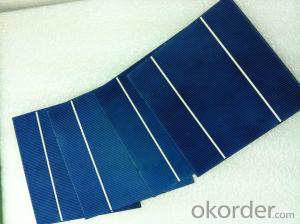
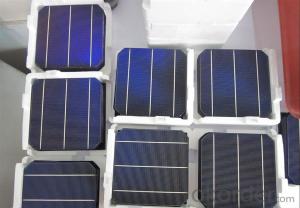
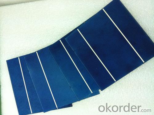


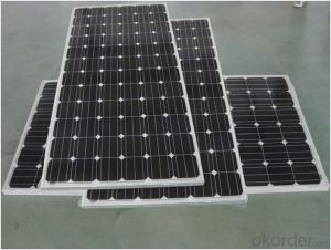
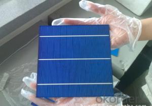
Solar Silicon Wafer Cassette Compatible High Current 17.2% Polycrystalline Silicon Solar Cell
- Ref Price:
-

- Loading Port:
- Shanghai
- Payment Terms:
- TT OR LC
- Min Order Qty:
- 1000 pc
- Supply Capability:
- 100000 pc/month
OKorder Service Pledge
OKorder Financial Service
You Might Also Like


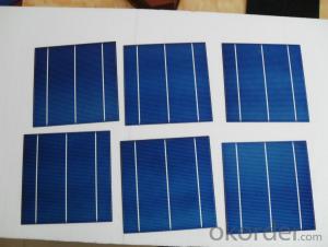
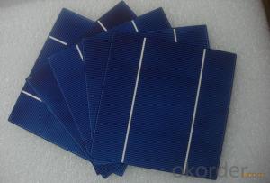
4 Bus Bars 156*156 17.6% efficiency poly solar cell
PHYSICAL CHARACTERISTICS
Dimension: 156mm x 156mm ± 0.5mm
Wafer Thickeness: 180um+20um and 200um+20um
Front(-) Four 1.2mm silver busbar
Silicon nitride blue anti-reflection coating
Back(+) aluminum back surface field
1.75mm(silver) wide segment soldering pads

Typical Electrical Characteristics
Efficiency | W(Pmpp) | V(Umpp) | A(Impp) | V(Uoc) | A(Isc) |
17.4-17.5 | 4.234 | 0.517 | 8.231 | 0.622 | 8.759 |
17.5-17.6 | 4.259 | 0.519 | 8.243 | 0.623 | 8.769 |
17.7-17.8 | 4.283 | 0.521 | 8.256 | 0.625 | 8.779 |
17.8-17.9 | 4.307 | 0.523 | 8.268 | 0.626 | 8.788 |
17.9-18.0 | 4.332 | 0.525 | 8.281 | 0.627 | 8.798 |
18.0-18.1 | 4.380 | 0.529 | 8.306 | 0.629 | 8.808 |
18.1-18.2 | 4.405 | 0.531 | 8.318 | 0.632 | 8.818 |
18.2-18.3 | 4.429 | 0.533 | 8.331 | 0.633 | 8.837 |
18.3-18.4 | 4.453 | 0.535 | 8.344 | 0.634 | 8.847 |
18.4-18.5 | 4.478 | 0.537 | 8.356 | 0.636 | 8.856 |
18.5-18.6 | 4.502 | 0.539 | 8.369 | 0.637 | 8.866 |
Efficiency | W(Pmpp) | V(Umpp) | A(Impp) | V(Uoc) | A(Isc) |
20.90-21.00 | 5.06 | 0.557 | 9.007 | 0.653 | 9.688 |
20.80-20.90 | 5.04 | 0.556 | 9.062 | 0.652 | 9.683 |
20.70-20.80 | 5.02 | 0.554 | 9.055 | 0.651 | 9.684 |
20.60-20.70 | 4.99 | 0.552 | 9.033 | 0.651 | 9.672 |
20.50-20.60 | 4.97 | 0.550 | 9.002 | 0.650 | 9.673 |
20.40-20.50 | 4.94 | 0.548 | 9.012 | 0.649 | 9.674 |
20.30-20.40 | 4.92 | 0.546 | 9.009 | 0.649 | 9.655 |
20.20-20.30 | 4.89 | 0.543 | 9.012 | 0.648 | 9.634 |
20.10-20.20 | 4.87 | 0.541 | 8.998 | 0.648 | 9.617 |
20.00-20.10 | 4.85 | 0.540 | 8.977 | 0.647 | 9.600 |
*Data under standard testing conditional (STC):1,000w/m2,AM1.5, 25°C , Pmax:Positive power tolerance.
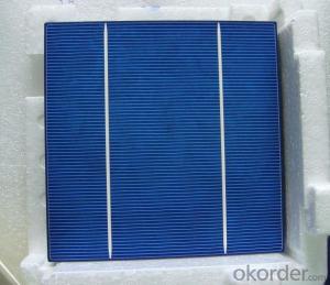
3 Bus Bars 156*156 17.4% efficiency poly solar cell
Dimension: 156 mm x 156 mm ± 0.5 mm
Wafer Thickeness: 156 mm x 156 mm ± 0.5 mm

Typical Electrical Characteristics:
| Efficiency code | 1660 | 1680 | 1700 | 1720 | 1740 | 1760 | 1780 | 1800 | 1820 | 1840 | 1860 |
| Efficiency (%) | 16.6 | 16.8 | 17.0 | 17.2 | 17.4 | 17.6 | 17.8 | 18.0 | 18.2 | 18.4 | 18.6 |
| Pmax (W) | 4.04 | 4.09 | 4.14 | 4.19 | 4.23 | 4.28 | 4.33 | 4.38 | 4.43 | 4.48 | 4.53 |
| Voc (V) | 0.612 | 0.615 | 0.618 | 0.621 | 0.624 | 0.627 | 0.629 | 0.63 | 0.633 | 0.635 | 0.637 |
| Isc (A) | 8.42 | 8.46 | 8.51 | 8.56 | 8.61 | 8.65 | 8.69 | 8.73 | 8.77 | 8.81 | 8.84 |
| Imp (A) | 7.91 | 7.99 | 8.08 | 8.16 | 8.22 | 8.27 | 8.33 | 8.38 | 8.43 | 8.48 | 8.53 |
* Testing conditions: 1000 W/m2, AM 1.5, 25 °C, Tolerance: Efficiency ± 0.2% abs., Pmpp ±1.5% rel.
* Imin : at 0.5 V
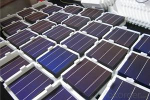
Production:

Package:

FAQ:
1. Q: Do you have your own factory?
A: Yes, we have. Our factory located in Jiangsu
2. Q: How can I visit your factory?
A: Before you visit,please contact us.We will show you the route or arrange a car to pick you up.
3. Q: Do you provide free sample?
A: Commenly we provide paid sample.
4. Q: Could you print our company LOGO on the nameplate and package?
A: Yes, we accept it.And need an Authorization Letter from you.
5. Q: Do you accept custom design on size?
A: Yes, if the size is reasonable.
6. Q: How can I be your agent in my country?
A: Please leave feedback. It's better for us to talk about details by email.
7. Q: Do you have solar project engineer who can guide me to install system?
A: Yes, we have a professional engineer team. They can teach you how to install a solar system.
- Q: What are the different materials used for backsheets in solar silicon wafers?
- The different materials used for backsheets in solar silicon wafers include polyester (PET), polyvinyl fluoride (PVF), and polyvinylidene fluoride (PVDF). These materials are chosen for their durability, weather resistance, and ability to protect the solar cells from moisture, UV radiation, and other environmental factors.
- Q: Can solar silicon wafers be used in solar-powered desalination plants?
- Yes, solar silicon wafers can be used in solar-powered desalination plants. These wafers are commonly used in photovoltaic (solar) panels to convert sunlight into electricity. By integrating solar silicon wafers into the desalination process, solar energy can be harnessed to power the plant's operations, reducing reliance on traditional energy sources and making the desalination process more sustainable.
- Q: What's the connection between silicon wafer and wafer
- Why is the semiconductor wafer has to be large because he wants to cut into small square chips
- Q: What are the main challenges in producing solar silicon wafers?
- The main challenges in producing solar silicon wafers include the high energy consumption during the production process, the high cost of raw materials and equipment, the need for high purity silicon, the complexity of the manufacturing process, and the environmental impact of the various chemical processes involved. Additionally, ensuring consistent quality control and minimizing defects in the wafers pose significant challenges to manufacturers.
- Q: What is the purpose of a degradation rate in a solar silicon wafer?
- The purpose of a degradation rate in a solar silicon wafer is to measure and predict the rate at which the wafer's performance or efficiency may decline over time due to various factors such as exposure to sunlight, temperature fluctuations, and environmental conditions. It helps in assessing the long-term durability and reliability of the solar panel, enabling manufacturers and users to make informed decisions about maintenance, warranty, and overall system performance.
- Q: What is the role of front contacts on solar silicon wafers?
- The role of front contacts on solar silicon wafers is to collect and extract the generated electricity from the solar cells. These contacts are typically made of metal fingers or grids that are placed on the front surface of the solar cell. They enable the flow of current and help in minimizing the resistance and losses, ensuring efficient electricity production from the solar panel.
- Q: Can solar silicon wafers be used in solar-powered drones?
- Yes, solar silicon wafers can be used in solar-powered drones. These wafers are commonly used in the production of solar cells and can efficiently convert sunlight into electricity. Solar-powered drones can utilize these wafers to generate the required energy for their operation, allowing them to fly for extended periods without relying on traditional fuel sources.
- Q: How do solar silicon wafers handle shading or partial obstructions?
- Solar silicon wafers are sensitive to shading or partial obstructions as they rely on receiving direct sunlight for optimal performance. When shaded, the affected area of the wafer generates less electricity, causing a decrease in overall energy output. This phenomenon is known as the "partial shading effect" and can significantly impact the efficiency of solar panels. To mitigate this, advanced solar panel designs incorporate bypass diodes that allow the electricity to bypass the shaded area, preventing a drop in overall power production. However, it is still recommended to install solar panels in locations with minimal shading or obstructions to ensure maximum energy generation.
- Q: Why do you use a concentrated sulfuric acid and hydrogen peroxide to wash silicon?
- Because of the use of sand when the recovery of mortar used too much, resulting in increased viscosity and organic impurities
- Q: Can solar silicon wafers be used in remote or inaccessible areas?
- Yes, solar silicon wafers can be used in remote or inaccessible areas. Solar panels made from silicon wafers are highly versatile and can be installed in various locations, even those that are remote or difficult to access. The panels can be transported and installed in these areas to harness solar energy effectively, providing a sustainable and reliable source of power.
Send your message to us
Solar Silicon Wafer Cassette Compatible High Current 17.2% Polycrystalline Silicon Solar Cell
- Ref Price:
-
- Loading Port:
- Shanghai
- Payment Terms:
- TT OR LC
- Min Order Qty:
- 1000 pc
- Supply Capability:
- 100000 pc/month
OKorder Service Pledge
OKorder Financial Service
Similar products


Hot products


Hot Searches
Related keywords

