
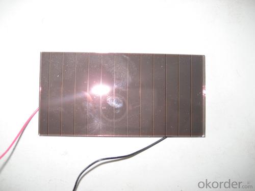
Solar Silicon Wafer - Amorphous Silicon Dice Specification 4
- Ref Price:
-

- Loading Port:
- China Main Port
- Payment Terms:
- TT OR LC
- Min Order Qty:
- -
- Supply Capability:
- -
OKorder Service Pledge
OKorder Financial Service
You Might Also Like


Pv modules at present, the mainstream products are still in silicon as the main raw materials, only in terms of silicon raw material consumption, production 1 mw of crystalline silicon solar cell, need 10 to 12 tons of high purity silicon, but if use the same silicon materials used to produce thin film amorphous silicon solar cell can produce more than 200 mw.
From the perspective of energy consumption, amorphous silicon solar battery only 1-1.5 years of energy recovery period, more embodies its contribution to energy saving in the manufacturing process.
Component occupies a high proportion of costs in a photovoltaic system, the component prices directly affect the system cost, and thus affect the cost of photovoltaic power generation. Calculated at the current price of components, the same money, buy amorphous silicon products, you can get more close to 30% of the power components.
2, more power
For the same power of solar cell array, amorphous silicon solar cell is about 10% more than monocrystalline silicon, polycrystalline silicon battery power. This has been the Uni - Solar System LLC, Energy Photovoltaic Corp., Japan's Kaneka Corp., the Netherlands Energy research institute, and other organizations and experts confirmed that the Photovoltaic industry.
In sunny, that is to say, under the high temperature, amorphous silicon solar cell components can show more excellent power performance.
3, better low light response
Due to the characteristics of amorphous silicon atoms are arranged disorderly, the electron transition no longer comply with the restriction of traditional \"selection rule\", as a result, its light absorption characteristics and there are big differences monocrystalline silicon material. Amorphous silicon and monocrystalline silicon material absorption curve as shown
, amorphous silicon absorption curve has obvious three sections (A, B, C). Area A corresponding electronic transition between localized states, such as the gap state near Fermi level and to the tail state transition, the absorption coefficient is small, about 1-10 cm - 1, for this is absorbing; B area absorption coefficient with the increase of the photon energy index rose, it corresponds to the electrons from the valence band edge extension state to the conduction band localized state transition, as well as the localized electrons from the valence band tail states guide for edge extension state transition, the region's energy range is usually only about half of the electron volts, but absorption coefficient across two or three orders of magnitude, usually up to 104 cm - 1; Area C corresponds to the electrons from the valence band to the conduction band internal internal transition, the absorption coefficient is bigger, often in more than 104 cm - 1. After two absorption area is crystalline silicon eigen absorption area.
Can be seen in the figure, the intersection of two curves about 1.8 ev. It is important to note that in the visible light range (1.7 to 3.0 ev), the absorption coefficient of amorphous silicon material is almost an order of magnitude larger than the single crystal silicon. That is to say, in the morning the first part of the sun is not too strong, the second half, and it's cloudy in the afternoon under the condition of low light intensity, long wave is greater, the amorphous silicon material still has a large absorption coefficient. Again considering the amorphous silicon band gap is larger, the reverse saturation current I0 is smaller. And as mentioned the amorphous silicon battery the characteristics I - V characteristic curve of the amorphous silicon solar cell both in theory and in practical use in low light intensity has good adaptation.
• I - V characteristics of amorphous silicon cells after more than a Vm with the voltage drop slowly
In order to be convenient, we draw the I - V characteristics of two kinds of batteries on the same picture. Crystalline silicon and amorphous silicon battery I - V characteristics of general shape as shown
we see from the picture, two kinds of cells in the curve changes after exceed the maximum output power point gap is bigger. Output current of crystalline silicon cells after exceed the maximum output power point will soon fall to zero, curve steep; Rather than crystalline silicon cells output current after a long distance to fall to zero, the curve is relatively flat. Two kinds of battery Vm equivalent to about 83% of its open circuit voltage and 83% respectively.
when light intensity gradually become hour, short circuit current and open circuit voltage of solar battery will be stronger. Short circuit current decreases faster, of course, open circuit voltage decrease more slowly.
do in battery solar cell array under the condition of load, when the sun battery array of effective output voltage less than the terminal voltage of battery, battery cannot be recharged. When the light intensity gradually become hour, crystal silicon battery charging does not meet the conditions, and amorphous silicon due to the larger voltage difference, do not charge until the light is very dark, effectively increase the use of sunlight time. So, amorphous silicon cells to produce more electricity than the crystalline silicon.
4, more excellent high temperature performance
High in the outdoor environment temperature, amorphous silicon solar cell performance change, depends on the temperature, spectrum, as well as other related factors. But what is certain is: amorphous silicon than monocrystalline silicon or polycrystalline silicon are less likely to be affected by temperature.
Amorphous silicon solar cells than monocrystalline silicon, polycrystalline silicon cells have relatively small temperature coefficient of amorphous silicon solar cell output power best Pm temperature coefficient is about 0.19%, and monocrystalline silicon, polycrystalline silicon cells best output power Pm temperature coefficient is about 0.5%, when the battery work at higher temperatures, the two batteries will be a drop in the Pm, but the decline is different. They can be calculated using the following formula.
- Q: How are solar silicon wafers interconnected to form solar modules?
- Solar silicon wafers are interconnected to form solar modules through a process called stringing and tabbing. This involves connecting multiple silicon wafers together using conductive wires or ribbons. The wafers are soldered or glued onto a backing material, and the conductive wires are then attached to the front and back contacts on each wafer, creating a series circuit. This interconnection allows the flow of electricity generated by each individual wafer to combine and be harnessed by the solar module as a whole.
- Q: How does the electrical conductivity affect the efficiency of a solar silicon wafer?
- The electrical conductivity of a solar silicon wafer directly affects its efficiency as it determines how well the wafer can transport the generated electrical charge. Higher electrical conductivity allows for better electron mobility, resulting in more efficient collection and transport of the generated electricity, thus increasing the overall efficiency of the solar cell.
- Q: How is the efficiency of a solar silicon wafer measured?
- The efficiency of a solar silicon wafer is typically measured by calculating the percentage of sunlight that is converted into usable electricity. This is done by dividing the power output of the solar cell by the power of the incident sunlight, and multiplying the result by 100 to get the efficiency percentage.
- Q: What is the meaning of a cleaning in a semiconductor silicon wafer process? RCA?
- () SPM:H2SO4 /H2O2 120 to 150 DEG C SPM has a high oxidation capacity, can be dissolved in the metal oxidation solution, and the oxidation of organic matter to generate CO 2 and H2O. The use of SPM to clean silicon wafers can remove heavy organic contaminants and some metals on the surface of silicon wafer, but it is difficult to remove organic matter when organic matter is particularly serious.
- Q: What is the typical size of a solar silicon wafer?
- The typical size of a solar silicon wafer is 156mm x 156mm or 6 inches x 6 inches.
- Q: How do solar silicon wafers perform in tropical environments?
- Solar silicon wafers perform well in tropical environments as they are designed to withstand high temperatures and humidity. The durable materials used in their construction can resist corrosion and degradation, ensuring their long-term performance and efficiency in such conditions.
- Q: Can solar silicon wafers be used in military applications?
- Yes, solar silicon wafers can be used in military applications. They can be integrated into various military technologies such as portable power systems, surveillance equipment, and remote communication devices to provide a reliable and sustainable source of energy in the field.
- Q: What is the role of solar silicon wafers in reducing the digital divide?
- Solar silicon wafers play a crucial role in reducing the digital divide by facilitating the production of affordable and sustainable solar panels. These panels can be used to generate electricity in remote and underserved areas where access to the power grid is limited. By harnessing solar energy, these communities can power devices such as computers, smartphones, and other digital technologies, thus bridging the gap in access to information and communication. Solar silicon wafers enable the production of cost-effective solar panels, expanding the reach of clean and renewable energy solutions, and contributing to narrowing the digital divide.
- Q: How does the cost of a solar silicon wafer compare to other types of solar cells?
- The cost of a solar silicon wafer is generally higher compared to other types of solar cells. Silicon-based solar cells have been widely used and have a mature manufacturing process, which helps to reduce costs. However, alternative solar cell technologies such as thin-film solar cells or organic solar cells have lower material costs and can be manufactured using less energy-intensive processes. These factors contribute to a lower overall cost for these types of solar cells compared to silicon wafers.
- Q: How to extract silicon from silicon wafers
- Annealing: double position hot oxidation furnace after nitrogen purging, infrared heating to 300~500 DEG C, silicon wafer surface and oxygen react, so that the surface of silicon dioxide protection layer.
Send your message to us
Solar Silicon Wafer - Amorphous Silicon Dice Specification 4
- Ref Price:
-
- Loading Port:
- China Main Port
- Payment Terms:
- TT OR LC
- Min Order Qty:
- -
- Supply Capability:
- -
OKorder Service Pledge
OKorder Financial Service
Similar products


Hot products


Hot Searches
Related keywords

