


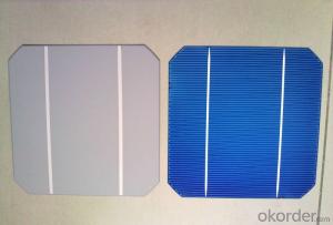
Solar Mono Silicon Wafer - Mono Solar Cells 156mm*156mm in Bulk Quantity Low Price Stock 19.2
- Ref Price:
-

- Loading Port:
- Shanghai
- Payment Terms:
- TT OR LC
- Min Order Qty:
- 1000 pc
- Supply Capability:
- 100000 pc/month
OKorder Service Pledge
OKorder Financial Service
You Might Also Like


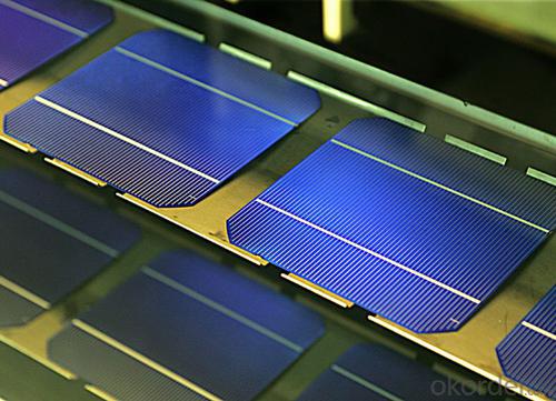
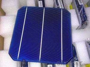
Brief Introduction
- Up to 20.0% efficiency, one of the highest performing mono crystalline cells on the market
- Three bus bars boosts current collection over the entire cell area, leading to higher fill factors
- Blue anti-reflecting coating allows more sunlight be captured and converted to electricity
- Finer, closer fingers improves charge collections for improved energy yield
- Lower light-induced degradation leads to greater power output over the entire module lifetime
- All solar cells are tightly classified to optimize output of module
- Maximum yield and longevity due to hotspot prevention
- Premium appearance results in a highly uniform and aesthetically appealing module
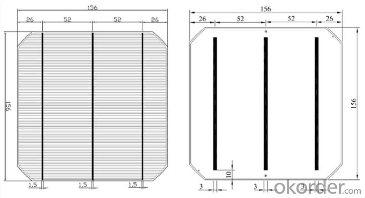
Specification
- Product Mono-crystalline silicon solar cell
- Dimension 156 mm x 156 mm ± 0.5 mm
- Thickness 200 μm ± 30 μm
- Front 1.5 ± 0.1 mm busbar (silver)
- Silicon nitride antireflection coating
- Back 3.0 mm continuous soldering pads (silver)
- Back surface field (aluminum)
Electric performance parameters

- Testing conditions: 1000 W/m2, AM 1.5, 25 °C, Tolerance: Efficiency ± 0.2% abs., Pmpp ±1.5% rel.
- Imin : at 0.5 V
Light Intensity Dependence

Soldering Ability
- Peel Strength: > 1.0 N/mm (Pull soldered ribbon from busbar in 5 mm/s of 180°)
Dimension Figure

Quick Response
- Any time and anywhere, reply clients' email and solve all problems happen in the work at the first time.
- Remove clients doubts and offer the best solution at the first time.
- Give our clients the lastest news of the photovoltaic, update the newest stock informtion.
Production and Quality Control
- Precision cell efficiency sorting procedures
- Stringent criteria for color uniformity and appearance
- Reverse current and shunt resistance screening
- ISO9001,ISO14001 and OHSAS 18001,TUV Certificated


FAQ:
1. Q: Do you have your own factory?
A: Yes, we have. Our factory located in Jiangsu
2. Q: How can I visit your factory?
A: Before you visit,please contact us.We will show you the route or arrange a car to pick you up.
3. Q: Do you provide free sample?
A: Commenly we provide paid sample.
4. Q: Could you print our company LOGO on the nameplate and package?
A: Yes, we accept it.And need an Authorization Letter from you.
5. Q: Do you accept custom design on size?
A: Yes, if the size is reasonable.
6. Q: How can I be your agent in my country?
A: Please leave feedback. It's better for us to talk about details by email.
7. Q: Do you have solar project engineer who can guide me to install system?
A: Yes, we have a professional engineer team. They can teach you how to install a solar system.
- Q: What is the role of back contact in solar silicon wafers?
- The role of back contact in solar silicon wafers is to provide electrical connection and support for the flow of current generated by the photovoltaic cells. It acts as a conductive layer that allows the captured solar energy to be efficiently transferred to external circuitry for use or storage. Additionally, it helps in maintaining the structural integrity of the wafer and protects the sensitive layers of the solar cell from external factors such as moisture and physical damage.
- Q: How do solar silicon wafers perform in cold climates?
- Solar silicon wafers perform well in cold climates as the low temperatures actually enhance their efficiency. The cold weather helps to reduce the resistance in the solar cells, allowing them to produce more electricity. However, extreme cold can lead to issues such as snow accumulation, which may temporarily hinder their performance until cleared. Overall, solar silicon wafers are designed to withstand and operate efficiently in cold weather conditions.
- Q: How has the technology for solar silicon wafers evolved over time?
- The technology for solar silicon wafers has evolved significantly over time. Initially, the production of silicon wafers involved a complex and expensive process, resulting in high costs for solar panels. However, advancements in manufacturing techniques and materials have led to improvements in efficiency and reduced costs. The size of the wafers has increased, allowing for more power generation per panel. Additionally, the quality of silicon used in the wafers has improved, enhancing the conversion of sunlight into electricity. Overall, these advancements have made solar energy more accessible and affordable for consumers and contributed to the growth of the renewable energy industry.
- Q: What is the expected cost reduction for solar silicon wafers in the future?
- It is difficult to provide an exact figure for the expected cost reduction of solar silicon wafers in the future as it depends on various factors such as technological advancements, economies of scale, and market demand. However, with ongoing research and development efforts in the solar industry, it is anticipated that the cost of silicon wafers will continue to decrease over time, making solar energy more affordable and accessible for consumers and businesses alike.
- Q: How to detect the surface finish of photovoltaic silicon wafers, what equipment?
- Do you want to check the surface roughness or do you want to clean it? These two are not the same,
- Q: Geometric parameters and testing of silicon wafer
- Silicon chips have side length 125mm, 156mm, and 125 of the large chamfer diagonal 156mm and small chamfer diagonal 165mm, polycrystalline silicon chip to the side of the 156mm based, diagonal 219.2mm.
- Q: Is solar silicon wafer often harmful to the body?
- Silicon is the main component of Si, is the most widely distributed on the earth, the most abundant storage materials
- Q: How is a spectral response measured in a solar silicon wafer?
- A spectral response in a solar silicon wafer is typically measured using a technique called external quantum efficiency (EQE) measurement. In this process, the wafer is illuminated with monochromatic light of varying wavelengths, and the resulting current generated by the solar cell is measured. The EQE measurement provides information about how efficiently the solar cell converts light of different wavelengths into electrical energy, allowing for a comprehensive understanding of the cell's spectral response.
- Q: How do solar silicon wafers perform in dusty environments?
- Solar silicon wafers can experience reduced performance in dusty environments due to the accumulation of dust particles on their surface. Dust can block sunlight and create a barrier between the wafer and the sunlight it needs to generate electricity. This can lead to a decrease in the efficiency of solar panels and a reduction in their overall power output. Regular cleaning and maintenance of solar panels in dusty environments is essential to ensure optimal performance.
- Q: What are the main factors that affect the lifespan of a solar silicon wafer?
- The main factors that affect the lifespan of a solar silicon wafer include the quality of the silicon material used, the manufacturing process, exposure to external factors such as temperature and humidity, and the level of stress the wafer is subjected to during operation. Additionally, proper handling, installation, and maintenance practices also play a significant role in determining the lifespan of a solar silicon wafer.
Send your message to us
Solar Mono Silicon Wafer - Mono Solar Cells 156mm*156mm in Bulk Quantity Low Price Stock 19.2
- Ref Price:
-
- Loading Port:
- Shanghai
- Payment Terms:
- TT OR LC
- Min Order Qty:
- 1000 pc
- Supply Capability:
- 100000 pc/month
OKorder Service Pledge
OKorder Financial Service
Similar products


Hot products


Hot Searches
Related keywords

