


Solar Silicon Wafer Cassette Supplier - High Quality A Grade Polycrystalline 5V 16.4% Solar Cell
- Ref Price:
-

- Loading Port:
- Shanghai
- Payment Terms:
- TT OR LC
- Min Order Qty:
- 1000 pc
- Supply Capability:
- 100000 pc/month
OKorder Service Pledge
OKorder Financial Service
You Might Also Like


Specifications
hot sale solar cell
1.16.8%~18.25% high efficiency
2.100% checked quality
3.ISO9001/ISO14001/TUV/CE/UL
4.stable performance
We can offer you the best quality products and services, don't miss !
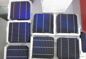
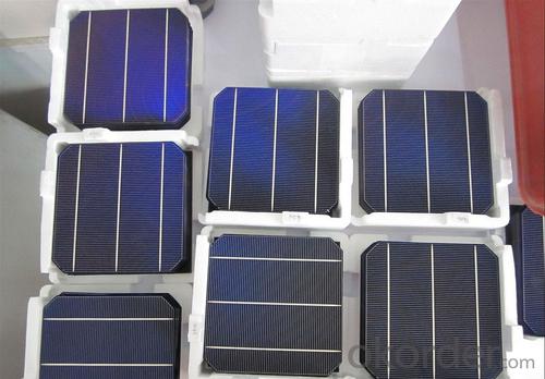
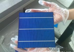
POLY6'(156*156)
Polycrystalline Silicon Solar cell
Physical Characteristics
Dimension: 156mm×156mm±0.5mm
Diagonal: 220mm±0.5mm
Thickness(Si): 200±20 μm
Front(-) Back(+)
Blue anti-reflecting coating (silicon nitride); Aluminum back surface field;
1.5mm wide bus bars; 2.0mm wide soldering pads;
Distance between bus bars: 51mm . Distance between bus bars :51mm .
Electrical Characteristics
Efficiency(%) | 18.00 | 17.80 | 17.60 | 17.40 | 17.20 | 16.80 | 16.60 | 16.40 | 16.20 | 16.00 | 15.80 | 15.60 |
Pmpp(W) | 4.33 | 4.29 | 4.24 | 4.19 | 4.14 | 4.09 | 4.04 | 3.99 | 3.94 | 3.90 | 3.86 | 3.82 |
Umpp(V) | 0.530 | 0.527 | 0.524 | 0.521 | 0.518 | 0.516 | 0.514 | 0.511 | 0.509 | 0.506 | 0.503 | 0.501 |
Impp(A) | 8.159 | 8.126 | 8.081 | 8.035 | 7.990 | 7.938 | 7.876 | 7.813 | 7.754 | 7.698 | 7.642 | 7.586 |
Uoc(V) | 0.633 | 0.631 | 0.628 | 0.625 | 0.623 | 0.620 | 0.618 | 0.617 | 0.615 | 0.613 | 0.611 | 0.609 |
Isc(A) | 8.709 | 8.677 | 8.629 | 8.578 | 8.531 | 8.478 | 8.419 | 8.356 | 8.289 | 8.220 | 8.151 | 8.083 |

MONO5'(125*125mm)165
Monocrystalline silicon solar cell
Physical Characteristics
Dimension: 125mm×125mm±0.5mm
Diagonal: 165mm±0.5mm
Thickness(Si): 200±20 μm
Front(-) Back(+)
Blue anti-reflecting coating(silicon nitride); Aluminum back surface field;
1.6mmwide bus bars; 2.5mm wide soldering pads;
Distance between bus bars: 61mm . Distance between bus bars :61mm .
Electrical Characteristics
Efficiency(%) | 19.40 | 19.20 | 19.00 | 18.80 | 18.60 | 18.40 | 18.20 | 18.00 | 17.80 | 17.60 | 17.40 | 17.20 |
Pmpp(W) | 2.97 | 2.94 | 2.91 | 2.88 | 2.85 | 2.82 | 2.79 | 2.76 | 2.73 | 2.70 | 2.67 | 2.62 |
Umpp(V) | 0.537 | 0.535 | 0.533 | 0.531 | 0.527 | 0.524 | 0.521 | 0.518 | 0.516 | 0.515 | 0.513 | 0.509 |
Impp(A) | 5.531 | 5.495 | 5.460 | 5.424 | 5.408 | 5.382 | 5.355 | 5.328 | 5.291 | 5.243 | 5.195 | 4.147 |
Uoc(V) | 0.637 | 0.637 | 0.636 | 0.635 | 0.633 | 0.630 | 0.629 | 0.629 | 0.628 | 0.626 | 0.626 | 0.625 |
Isc(A) | 5.888 | 5.876 | 5.862 | 5.848 | 5.839 | 5.826 | 5.809 | 5.791 | 5.779 | 5.756 | 5.293 | 5.144 |

FAQ:
Q:How can i get some sample?
A:Yes , if you want order ,sample is not a problem.
Q:How about your solar panel efficency?
A: Our product efficency around 17.25%~18.25%.
Q:What’s the certificate you have got?
A: we have overall product certificate of ISO9001/ISO14001/CE/TUV/UL
- Q: What is the role of surface recombination velocity on solar silicon wafers?
- The surface recombination velocity on solar silicon wafers plays a crucial role in determining the efficiency of solar cells. It represents the rate at which charge carriers (electrons and holes) recombine at the surface of the wafer. A low surface recombination velocity is desirable as it reduces the recombination losses, allowing more charge carriers to reach the contacts and contribute to the electricity generation. Therefore, optimizing and minimizing the surface recombination velocity is essential for improving the performance of solar cells and increasing their overall efficiency.
- Q: How is the bandgap of a solar silicon wafer determined?
- The bandgap of a solar silicon wafer is determined by measuring the energy difference between the valence band and the conduction band using techniques such as optical absorption spectroscopy or photoluminescence spectroscopy.
- Q: What is a good solar wafer testing equipment?
- To develop solar energy, we must overcome two key challenges: cost and yield." In the solar panel manufacturing process, from the front to the back, from the crystal rod, wafer, chip to the module, any one of the links in error, will affect the number of solar panel products. Therefore, the solar cell needs to be able to monitor every step of the process in the production process of detection tools. QCROBOT also has many successful cases in this field.
- Q: What is the thickness of the semiconductor wafer used today?I have consulted some for solar wafers, heard now that the wafer thickness in 200~400 micron, but we need the wafer thickness requirements for high now, that for semiconductor wafer thickness is slightly higher than the solar energy, but I do not know how much is there in about 1 mm
- We do DIP package, 4 inch wafer to be thin to 0.300mm; 6 inch wafer to be reduced to about 0.320mm, error 0.020mm.
- Q: What are the different types of mounting structures used for solar silicon wafers?
- There are mainly three types of mounting structures used for solar silicon wafers: fixed mounts, tracking mounts, and floating mounts. Fixed mounts are stationary structures that hold the solar panels in a fixed position facing the sun. Tracking mounts, on the other hand, are designed to follow the movement of the sun throughout the day, maximizing the amount of sunlight captured by the panels. Lastly, floating mounts are used for solar panels placed on water bodies, such as lakes or reservoirs, allowing for efficient use of space and reducing land requirements.
- Q: What is the purity level of the silicon used in solar silicon wafers?
- The purity level of the silicon used in solar silicon wafers is typically very high, with a purity level of 99.9999% (6N) or even higher.
- Q: What is the role of light trapping in solar silicon wafers?
- The role of light trapping in solar silicon wafers is to increase the absorption of sunlight within the wafer, thereby enhancing the overall efficiency of the solar cell. By incorporating light trapping structures or techniques, such as textured surfaces or anti-reflective coatings, more light is effectively captured and confined within the wafer, allowing for a greater number of photons to be converted into electricity. This improves the performance of the solar cell by maximizing the utilization of available sunlight.
- Q: After wafer cleaning, how to change the film?
- Quality solutionCleaning method(a) RCA cleaning:RCA pioneered by Werner Kern in the N.J.Princeton RCA laboratory in 1965, and hence the name.RCA cleaning is a typical wet chemical cleaning.RCA cleaning is mainly used for cleaning the surface film, organic particles and metal contamination.1, particle cleaningThe main APM removal of silicon surface particles (also known as SC1) cleaning solution (NH4OH + H2O2 + H2O) to APM in the cleaning. The cleaning solution, due to the effects of H2O2, the silicon surface has a layer of natural oxide film (SiO2), a hydrophilic surface and between silicon particles can soaking cleaning liquid, silicon surface the natural oxide film and a silicon wafer surface by NH4OH corrosion, the particles will fall into the cleaning solution. The corrosion rate and the particle removal amount of silicon surface, for removing particles, corrosion must be a certain amount. In the cleaning solution, because the potential of silicon surface is negative, and most of the particles are repulsive force to prevent the adsorption of particles to the silicon surface.
- Q: How do solar silicon wafers convert sunlight into electricity?
- Solar silicon wafers convert sunlight into electricity through a process called the photovoltaic effect. When sunlight hits the silicon wafer, it excites the electrons in the material, causing them to break free from their atoms. These free electrons then flow through the wafer, creating an electric current. The wafer is designed with carefully placed layers of different materials, allowing the separation and collection of the generated electrons, ultimately producing usable electricity.
- Q: Can solar silicon wafers be used in tandem solar cell configurations?
- Yes, solar silicon wafers can be used in tandem solar cell configurations. Tandem solar cells involve stacking multiple solar cells with different bandgaps to increase the overall efficiency of the solar module. Silicon wafers are commonly used as one of the materials in tandem solar cells due to their abundance and cost-effectiveness.
Send your message to us
Solar Silicon Wafer Cassette Supplier - High Quality A Grade Polycrystalline 5V 16.4% Solar Cell
- Ref Price:
-
- Loading Port:
- Shanghai
- Payment Terms:
- TT OR LC
- Min Order Qty:
- 1000 pc
- Supply Capability:
- 100000 pc/month
OKorder Service Pledge
OKorder Financial Service
Similar products


Hot products


Hot Searches
Related keywords

