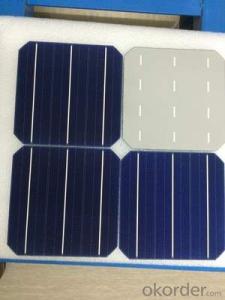

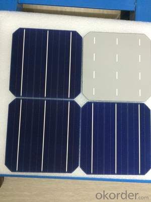


Silicon Wafer Solar Panel - Mono Solar Cells 156mm*156mm in Bulk Quantity Low Price Stock 20.0
- Ref Price:
-

- Loading Port:
- Shanghai
- Payment Terms:
- TT OR LC
- Min Order Qty:
- 1000 pc
- Supply Capability:
- 100000 pc/month
OKorder Service Pledge
OKorder Financial Service
You Might Also Like


Brief Introduction
- Up to 20.0% efficiency, one of the highest performing mono crystalline cells on the market
- Three bus bars boosts current collection over the entire cell area, leading to higher fill factors
- Blue anti-reflecting coating allows more sunlight be captured and converted to electricity
- Finer, closer fingers improves charge collections for improved energy yield
- Lower light-induced degradation leads to greater power output over the entire module lifetime
- All solar cells are tightly classified to optimize output of module
- Maximum yield and longevity due to hotspot prevention
- Premium appearance results in a highly uniform and aesthetically appealing module
Specification
- Product Mono-crystalline silicon solar cell
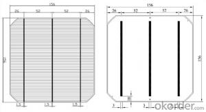
- Dimension 156 mm x 156 mm ± 0.5 mm
- Thickness 200 μm ± 30 μm
- Front 1.5 ± 0.1 mm busbar (silver)
- Silicon nitride antireflection coating
- Back 3.0 mm continuous soldering pads (silver)
- Back surface field (aluminum)
Electric performance parameters

- Testing conditions: 1000 W/m2, AM 1.5, 25 °C, Tolerance: Efficiency ± 0.2% abs., Pmpp ±1.5% rel.
- Imin : at 0.5 V
Light Intensity Dependence

Soldering Ability
- Peel Strength: > 1.0 N/mm (Pull soldered ribbon from busbar in 5 mm/s of 180°)
Dimension Figure

Quick Response
- Any time and anywhere, reply clients' email and solve all problems happen in the work at the first time.
- Remove clients doubts and offer the best solution at the first time.
- Give our clients the lastest news of the photovoltaic, update the newest stock informtion.
Production and Quality Control
- Precision cell efficiency sorting procedures
- Stringent criteria for color uniformity and appearance
- Reverse current and shunt resistance screening
- ISO9001,ISO14001 and OHSAS 18001,TUV Certificated


FAQ:
1. Q: Do you have your own factory?
A: Yes, we have. Our factory located in Jiangsu
2. Q: How can I visit your factory?
A: Before you visit,please contact us.We will show you the route or arrange a car to pick you up.
3. Q: Do you provide free sample?
A: Commenly we provide paid sample.
4. Q: Could you print our company LOGO on the nameplate and package?
A: Yes, we accept it.And need an Authorization Letter from you.
5. Q: Do you accept custom design on size?
A: Yes, if the size is reasonable.
6. Q: How can I be your agent in my country?
A: Please leave feedback. It's better for us to talk about details by email.
7. Q: Do you have solar project engineer who can guide me to install system?
A: Yes, we have a professional engineer team. They can teach you how to install a solar system.
- Q: Are solar silicon wafers affected by vibrations?
- Yes, solar silicon wafers can be affected by vibrations. Vibrations can cause microcracks or damage to the delicate structure of the wafer, reducing its efficiency and overall performance. It is important to handle and install solar silicon wafers with care to minimize the risk of damage from vibrations.
- Q: Are there any advancements in solar silicon wafer technology?
- Yes, there have been significant advancements in solar silicon wafer technology. Researchers and manufacturers have been working on improving the efficiency and cost-effectiveness of silicon wafers used in solar cells. Some advancements include the development of thin-film silicon wafers, which require less material and energy during production, and the incorporation of new materials and processes to enhance the conversion efficiency of solar cells. These advancements aim to make solar energy more affordable and accessible for a wider range of applications.
- Q: How are solar silicon wafers protected from vandalism or intentional damage?
- Solar silicon wafers are typically protected from vandalism or intentional damage through various measures. One common method is to install them within secure enclosures or fenced areas, making it difficult for unauthorized individuals to physically access and tamper with them. Additionally, surveillance systems such as CCTV cameras may be deployed to monitor the vicinity and deter potential vandals. In some cases, alarm systems or motion sensors are also employed to alert authorities in case of any suspicious activity. These measures, combined with proper signage indicating the presence of a protected solar installation, contribute towards safeguarding solar silicon wafers from vandalism or intentional damage.
- Q: How is a front contact applied to a solar silicon wafer?
- A front contact is typically applied to a solar silicon wafer through a process known as screen printing. In this process, a conductive paste containing metal particles is applied to the front surface of the wafer using a fine mesh screen. The paste is then dried and fired at high temperatures, causing the metal particles to fuse together and form a continuous conductive layer. This front contact acts as an electrode, allowing the collection and extraction of the generated electrical current from the solar cell.
- Q: What is the size of a typical solar silicon wafer?
- A typical solar silicon wafer is typically around 156mm (6.14 inches) in size.
- Q: What is a silicon wafer
- Silicon is an important material in the IC fabrication, through photolithography and ion implantation on the silicon wafer and other means, can be made into various semiconductor devices made of silicon chip. With amazing computational capabilities. The development of science and technology promotes the development of semiconductor. Development of automation and computer technology, this makes the silicon chip (integrated circuit) high technology product cost has been reduced to a very low degree. This makes the silicon wafer has been widely used in aerospace, industry, agriculture and national defense, and even crept into every family.
- Q: What is the impact of impurities on the durability of solar silicon wafers?
- Impurities in solar silicon wafers can have a significant impact on their durability. These impurities can affect the structural integrity and electrical properties of the wafers, leading to reduced efficiency and shorter lifespan of the solar cells. Impurities like metal ions or oxygen can introduce defects in the crystal lattice, causing degradation and increased recombination of charge carriers. This can result in reduced power output and decreased overall performance of the solar panels. Therefore, minimizing impurities and ensuring high purity silicon is crucial for enhancing the durability and longevity of solar silicon wafers.
- Q: Can solar silicon wafers be used in solar-powered agricultural applications?
- Yes, solar silicon wafers can be used in solar-powered agricultural applications. These wafers are commonly used in solar panels to convert sunlight into electricity. In agricultural applications, solar-powered systems can be used for various purposes such as irrigation, greenhouse lighting, and powering farm equipment. By utilizing solar silicon wafers, farmers can harness clean and renewable energy to enhance their farming operations while reducing reliance on traditional energy sources.
- Q: How long do solar silicon wafers last in a solar panel?
- Solar silicon wafers can last for several decades in a solar panel, typically around 25 to 30 years.
- Q: What are the different sizes available for solar silicon wafers?
- Solar silicon wafers are available in various sizes, commonly ranging from 125mm to 300mm in diameter.
Send your message to us
Silicon Wafer Solar Panel - Mono Solar Cells 156mm*156mm in Bulk Quantity Low Price Stock 20.0
- Ref Price:
-
- Loading Port:
- Shanghai
- Payment Terms:
- TT OR LC
- Min Order Qty:
- 1000 pc
- Supply Capability:
- 100000 pc/month
OKorder Service Pledge
OKorder Financial Service
Similar products


Hot products


Hot Searches
Related keywords

