


Silicon Wafer in Solar Photovoltaic Cells - Mono Solar Cells 156mm*156mm in Bulk Quantity Low Price Stock 19.8
- Ref Price:
-

- Loading Port:
- Shanghai
- Payment Terms:
- TT OR LC
- Min Order Qty:
- 1000 pc
- Supply Capability:
- 100000 pc/month
OKorder Service Pledge
OKorder Financial Service
You Might Also Like


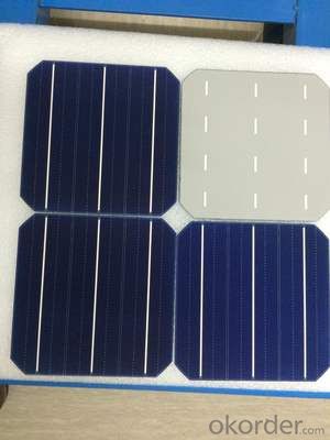
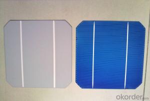
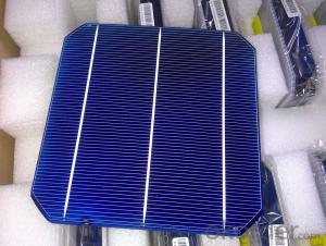
Brief Introduction
- Up to 20.0% efficiency, one of the highest performing mono crystalline cells on the market
- Three bus bars boosts current collection over the entire cell area, leading to higher fill factors
- Blue anti-reflecting coating allows more sunlight be captured and converted to electricity
- Finer, closer fingers improves charge collections for improved energy yield
- Lower light-induced degradation leads to greater power output over the entire module lifetime
- All solar cells are tightly classified to optimize output of module
- Maximum yield and longevity due to hotspot prevention
- Premium appearance results in a highly uniform and aesthetically appealing module
Specification
- Product Mono-crystalline silicon solar cell
- Dimension 156 mm x 156 mm ± 0.5 mm
- Thickness 200 μm ± 30 μm
- Front 1.5 ± 0.1 mm busbar (silver)
- Silicon nitride antireflection coating
- Back 3.0 mm continuous soldering pads (silver)
- Back surface field (aluminum)
Electric performance parameters

- Testing conditions: 1000 W/m2, AM 1.5, 25 °C, Tolerance: Efficiency ± 0.2% abs., Pmpp ±1.5% rel.
- Imin : at 0.5 V
Light Intensity Dependence

Soldering Ability
- Peel Strength: > 1.0 N/mm (Pull soldered ribbon from busbar in 5 mm/s of 180°)
Dimension Figure

Quick Response
- Any time and anywhere, reply clients' email and solve all problems happen in the work at the first time.
- Remove clients doubts and offer the best solution at the first time.
- Give our clients the lastest news of the photovoltaic, update the newest stock informtion.
Production and Quality Control
- Precision cell efficiency sorting procedures
- Stringent criteria for color uniformity and appearance
- Reverse current and shunt resistance screening
- ISO9001,ISO14001 and OHSAS 18001,TUV Certificated


FAQ:
1. Q: Do you have your own factory?
A: Yes, we have. Our factory located in Jiangsu
2. Q: How can I visit your factory?
A: Before you visit,please contact us.We will show you the route or arrange a car to pick you up.
3. Q: Do you provide free sample?
A: Commenly we provide paid sample.
4. Q: Could you print our company LOGO on the nameplate and package?
A: Yes, we accept it.And need an Authorization Letter from you.
5. Q: Do you accept custom design on size?
A: Yes, if the size is reasonable.
6. Q: How can I be your agent in my country?
A: Please leave feedback. It's better for us to talk about details by email.
7. Q: Do you have solar project engineer who can guide me to install system?
A: Yes, we have a professional engineer team. They can teach you how to install a solar system.
- Q: Are solar silicon wafers affected by vibrations?
- Yes, solar silicon wafers can be affected by vibrations. Vibrations can cause microcracks or damage to the delicate structure of the wafer, reducing its efficiency and overall performance. It is important to handle and install solar silicon wafers with care to minimize the risk of damage from vibrations.
- Q: What is the role of solar silicon wafers in reducing carbon emissions?
- Solar silicon wafers play a crucial role in reducing carbon emissions by serving as the key component in manufacturing solar panels. These wafers, made from highly purified silicon, absorb sunlight and convert it into clean, renewable electricity through the photovoltaic effect. By harnessing solar energy, we can reduce our reliance on fossil fuels and traditional power sources that emit greenhouse gases, thus significantly lowering carbon emissions and mitigating climate change.
- Q: Can solar silicon wafers be repaired?
- Yes, solar silicon wafers can be repaired to a certain extent. Small damages such as microcracks or scratches can often be repaired using various techniques, including polishing or laser-based methods. However, more significant damages, such as large cracks or broken wafers, may require replacement rather than repair.
- Q: How is an anti-reflective coating applied to a solar silicon wafer?
- An anti-reflective coating is typically applied to a solar silicon wafer through a process called chemical vapor deposition (CVD). In this process, a thin layer of silicon nitride or silicon oxide is deposited onto the wafer's surface. This coating helps to reduce reflection and increase light absorption, thereby improving the efficiency of the solar cell.
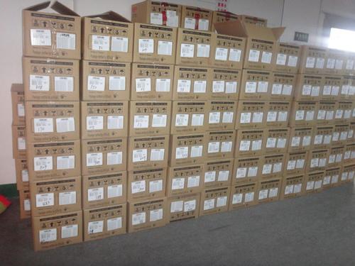
- Q: How are solar silicon wafers protected from transportation damage?
- Solar silicon wafers are protected from transportation damage through the use of specialized packaging materials and handling procedures. These wafers are typically placed in anti-static trays or boxes, which provide cushioning and prevent physical impact during transit. Additionally, shock-absorbing materials such as foam or bubble wrap may be used to further protect the wafers from vibrations or jolts. Furthermore, stringent quality control measures are implemented to ensure that the packaging is secure and that the wafers are not exposed to extreme temperatures or humidity, which could potentially damage their delicate structure.
- Q: What is the purpose of a fill factor in a solar silicon wafer?
- The purpose of a fill factor in a solar silicon wafer is to measure the efficiency of the solar cell. It represents the ratio of the maximum power output of the solar cell to the product of the open-circuit voltage and short-circuit current. A higher fill factor indicates a more efficient solar cell, as it signifies a better utilization of the available solar energy.
- Q: Are solar silicon wafers affected by power grid fluctuations?
- No, solar silicon wafers are not directly affected by power grid fluctuations. Solar panels generate electricity independently of the power grid, using sunlight to produce energy. However, fluctuations in the power grid can indirectly impact the overall efficiency and performance of solar panels, as they rely on a stable grid connection for grid-tied systems or for energy storage purposes.
- Q: What is the thickness of a solar silicon wafer?
- The thickness of a solar silicon wafer typically ranges from 150 to 200 micrometers (µm).
- Q: What is the typical efficiency range of solar silicon wafers?
- The typical efficiency range of solar silicon wafers is between 15% to 22%.
- Q: What is the average reflectivity of a solar silicon wafer?
- The average reflectivity of a solar silicon wafer is typically around 30%.
Send your message to us
Silicon Wafer in Solar Photovoltaic Cells - Mono Solar Cells 156mm*156mm in Bulk Quantity Low Price Stock 19.8
- Ref Price:
-
- Loading Port:
- Shanghai
- Payment Terms:
- TT OR LC
- Min Order Qty:
- 1000 pc
- Supply Capability:
- 100000 pc/month
OKorder Service Pledge
OKorder Financial Service
Similar products


Hot products


Hot Searches
Related keywords

