


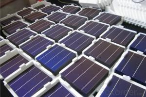
Silicon Wafer in Solar Cell - High Quality A Grade Mono Crystalline 5V 18.0% Solar Cell
- Ref Price:
-

- Loading Port:
- Shanghai
- Payment Terms:
- TT OR LC
- Min Order Qty:
- 1000 pc
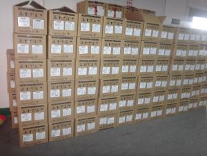
- Supply Capability:
- 100000 pc/month
OKorder Service Pledge
OKorder Financial Service
You Might Also Like


Specifications
hot sale solar cell
1.16.8%~18.25% high efficiency
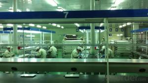
2.100% checked quality
3.ISO9001/ISO14001/TUV/CE/UL
4.stable performance
We can offer you the best quality products and services, don't miss !
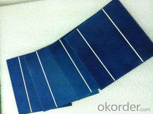
POLY6'(156*156)
Polycrystalline Silicon Solar cell
Physical Characteristics
Dimension: 156mm×156mm±0.5mm
Diagonal: 220mm±0.5mm
Thickness(Si): 200±20 μm
Front(-) Back(+)
Blue anti-reflecting coating (silicon nitride); Aluminum back surface field;
1.5mm wide bus bars; 2.0mm wide soldering pads;
Distance between bus bars: 51mm . Distance between bus bars :51mm .
Electrical Characteristics
Efficiency(%) | 18.00 | 17.80 | 17.60 | 17.40 | 17.20 | 16.80 | 16.60 | 16.40 | 16.20 | 16.00 | 15.80 | 15.60 |
Pmpp(W) | 4.33 | 4.29 | 4.24 | 4.19 | 4.14 | 4.09 | 4.04 | 3.99 | 3.94 | 3.90 | 3.86 | 3.82 |
Umpp(V) | 0.530 | 0.527 | 0.524 | 0.521 | 0.518 | 0.516 | 0.514 | 0.511 | 0.509 | 0.506 | 0.503 | 0.501 |
Impp(A) | 8.159 | 8.126 | 8.081 | 8.035 | 7.990 | 7.938 | 7.876 | 7.813 | 7.754 | 7.698 | 7.642 | 7.586 |
Uoc(V) | 0.633 | 0.631 | 0.628 | 0.625 | 0.623 | 0.620 | 0.618 | 0.617 | 0.615 | 0.613 | 0.611 | 0.609 |
Isc(A) | 8.709 | 8.677 | 8.629 | 8.578 | 8.531 | 8.478 | 8.419 | 8.356 | 8.289 | 8.220 | 8.151 | 8.083 |

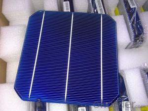
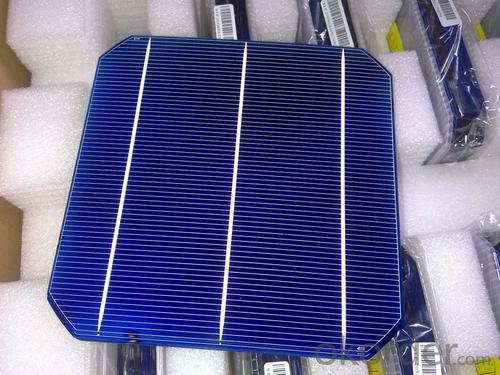
MONO5'(125*125mm)165
Monocrystalline silicon solar cell
Physical Characteristics
Dimension: 125mm×125mm±0.5mm
Diagonal: 165mm±0.5mm
Thickness(Si): 200±20 μm
Front(-) Back(+)
Blue anti-reflecting coating(silicon nitride); Aluminum back surface field;
1.6mmwide bus bars; 2.5mm wide soldering pads;
Distance between bus bars: 61mm . Distance between bus bars :61mm .
Electrical Characteristics
Efficiency(%) | 19.40 | 19.20 | 19.00 | 18.80 | 18.60 | 18.40 | 18.20 | 18.00 | 17.80 | 17.60 | 17.40 | 17.20 |
Pmpp(W) | 2.97 | 2.94 | 2.91 | 2.88 | 2.85 | 2.82 | 2.79 | 2.76 | 2.73 | 2.70 | 2.67 | 2.62 |
Umpp(V) | 0.537 | 0.535 | 0.533 | 0.531 | 0.527 | 0.524 | 0.521 | 0.518 | 0.516 | 0.515 | 0.513 | 0.509 |
Impp(A) | 5.531 | 5.495 | 5.460 | 5.424 | 5.408 | 5.382 | 5.355 | 5.328 | 5.291 | 5.243 | 5.195 | 4.147 |
Uoc(V) | 0.637 | 0.637 | 0.636 | 0.635 | 0.633 | 0.630 | 0.629 | 0.629 | 0.628 | 0.626 | 0.626 | 0.625 |
Isc(A) | 5.888 | 5.876 | 5.862 | 5.848 | 5.839 | 5.826 | 5.809 | 5.791 | 5.779 | 5.756 | 5.293 | 5.144 |

FAQ:
Q:How can i get some sample?
A:Yes , if you want order ,sample is not a problem.
Q:How about your solar panel efficency?
A: Our product efficency around 17.25%~18.25%.
Q:What’s the certificate you have got?
A: we have overall product certificate of ISO9001/ISO14001/CE/TUV/UL
- Q: Are there any initiatives to reduce the environmental impact of solar silicon wafer production?
- Yes, there are various initiatives aimed at reducing the environmental impact of solar silicon wafer production. These include the development and adoption of more sustainable manufacturing processes, such as the use of renewable energy sources in production facilities, reducing water usage, and implementing recycling programs for waste materials. Additionally, research is being conducted to explore alternative materials and techniques that could further minimize the environmental footprint of solar silicon wafer production.
- Q: Can solar silicon wafers be used in solar-powered military applications?
- Yes, solar silicon wafers can be used in solar-powered military applications. Solar silicon wafers are a key component in solar panels, which can be utilized to power a variety of military equipment, such as remote surveillance systems, communications equipment, and even portable power sources for soldiers in the field. The use of solar power in military applications offers numerous benefits, including reduced reliance on traditional fuel sources, increased energy efficiency, and enhanced operational sustainability.
- Q: Are solar silicon wafers flexible?
- No, solar silicon wafers are not flexible. They are rigid and typically made from crystalline silicon, which is a brittle material.
- Q: How is the purity of silicon determined for solar wafers?
- The purity of silicon for solar wafers is determined through various analytical techniques such as mass spectrometry, spectroscopy, and resistivity measurement. These methods help identify and quantify impurities like metals, oxygen, carbon, and other elements that may affect the efficiency and performance of the solar cells. Additionally, advanced purification processes are employed to ensure the highest level of purity, resulting in highly efficient solar wafers for photovoltaic applications.
- Q: How are solar silicon wafers connected within a solar panel?
- Solar silicon wafers are typically connected within a solar panel using metal conductive strips that are soldered to the front and back surfaces of the wafers. These conductive strips form electrical connections between the individual wafers, allowing the flow of current generated by sunlight to be harnessed and utilized efficiently.
- Q: What is the impact of wafer resistivity on solar silicon wafer performance?
- The wafer resistivity has a significant impact on the performance of solar silicon wafers. Lower resistivity wafers allow for better electrical conductivity, resulting in improved charge carrier mobility. This leads to higher efficiency in converting sunlight into electricity. Additionally, lower resistivity helps minimize power losses and enhances the overall performance and output of solar cells.
- Q: What are the different types of solar silicon wafers available?
- There are mainly three types of solar silicon wafers available: monocrystalline, polycrystalline, and thin-film. Monocrystalline wafers are made from a single crystal structure, providing high efficiency but at a higher cost. Polycrystalline wafers are made from multiple crystal structures, offering slightly lower efficiency but at a more affordable price. Thin-film wafers are made by depositing a thin layer of semiconductor material onto a substrate, providing flexibility and lower manufacturing costs, but with lower efficiency compared to crystalline wafers.
- Q: How many watts can a piece of silicon produce
- A piece of silicon, has been able to integrate 160 thousand transistors. What a fine project! This is the crystallization of multidisciplinary collaborative efforts, is another milestone in the progress of science and technology.
- Q: Are solar silicon wafers affected by voltage fluctuations?
- Yes, solar silicon wafers can be affected by voltage fluctuations. Fluctuations in voltage can impact the performance and efficiency of solar cells, potentially leading to decreased power output. It is important to maintain stable and consistent voltage levels to optimize the performance of solar panels.
- Q: How are solar silicon wafers protected from thermal damage?
- Solar silicon wafers are protected from thermal damage through various methods. One common technique is the use of passivation layers, such as silicon nitride or silicon oxide, which act as a protective coating to prevent heat-induced degradation. These layers help to reduce surface recombination and enhance the overall efficiency of the solar cell. Additionally, the wafers may be encapsulated within a transparent and heat-resistant material, such as glass or polymer, which provides insulation and safeguards against thermal stress. Careful design and engineering of the solar cell structure also contribute to efficient heat dissipation, ensuring that the wafers can withstand high temperatures without sustaining damage.
Send your message to us
Silicon Wafer in Solar Cell - High Quality A Grade Mono Crystalline 5V 18.0% Solar Cell
- Ref Price:
-
- Loading Port:
- Shanghai
- Payment Terms:
- TT OR LC
- Min Order Qty:
- 1000 pc
- Supply Capability:
- 100000 pc/month
OKorder Service Pledge
OKorder Financial Service
Similar products

Hot products


Hot Searches
Related keywords

