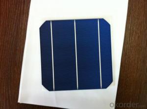
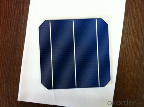
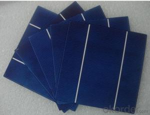
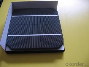
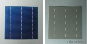
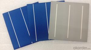
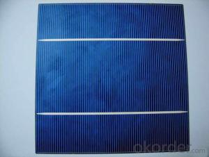
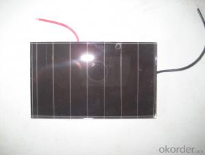
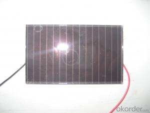
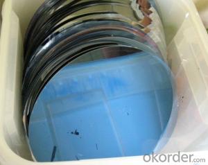
Multicrystalline Silicon Solar Wafer - High Quality A Grade Poly/Monocrystalline 5V Solar Cell
- Loading Port:
- Shanghai
- Payment Terms:
- TT OR LC
- Min Order Qty:
- 1000 pc
- Supply Capability:
- 100000 pc/month
OKorder Service Pledge
OKorder Financial Service
You Might Also Like
Specifications
hot sale solar cell
1.16.8%~18.25% high efficiency
2.100% checked quality
3.ISO9001/ISO14001/TUV/CE/UL
4.stable performance
We can offer you the best quality products and services, don't miss !
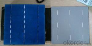
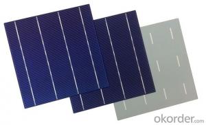
POLY6'(156*156)
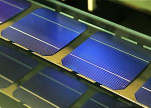
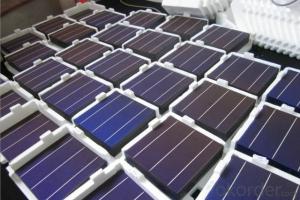
Polycrystalline Silicon Solar cell
Physical Characteristics
Dimension: 156mm×156mm±0.5mm
Diagonal: 220mm±0.5mm
Thickness(Si): 200±20 μm
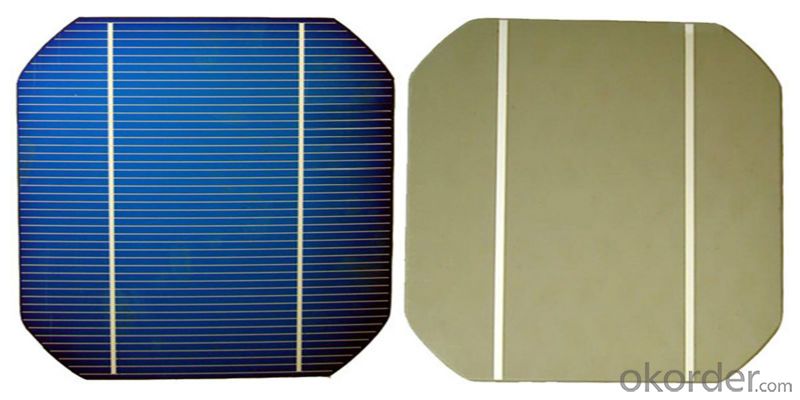
Front(-) Back(+)
Blue anti-reflecting coating (silicon nitride); Aluminum back surface field;
1.5mm wide bus bars; 2.0mm wide soldering pads;
Distance between bus bars: 51mm . Distance between bus bars :51mm .
Electrical Characteristics
Efficiency(%) | 18.00 | 17.80 | 17.60 | 17.40 | 17.20 | 16.80 | 16.60 | 16.40 | 16.20 | 16.00 | 15.80 | 15.60 |
Pmpp(W) | 4.33 | 4.29 | 4.24 | 4.19 | 4.14 | 4.09 | 4.04 | 3.99 | 3.94 | 3.90 | 3.86 | 3.82 |
Umpp(V) | 0.530 | 0.527 | 0.524 | 0.521 | 0.518 | 0.516 | 0.514 | 0.511 | 0.509 | 0.506 | 0.503 | 0.501 |
Impp(A) | 8.159 | 8.126 | 8.081 | 8.035 | 7.990 | 7.938 | 7.876 | 7.813 | 7.754 | 7.698 | 7.642 | 7.586 |
Uoc(V) | 0.633 | 0.631 | 0.628 | 0.625 | 0.623 | 0.620 | 0.618 | 0.617 | 0.615 | 0.613 | 0.611 | 0.609 |
Isc(A) | 8.709 | 8.677 | 8.629 | 8.578 | 8.531 | 8.478 | 8.419 | 8.356 | 8.289 | 8.220 | 8.151 | 8.083 |
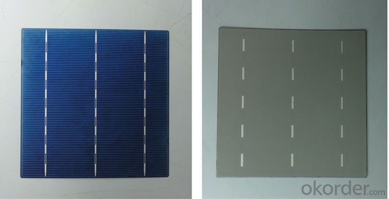
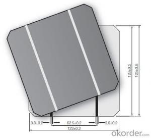
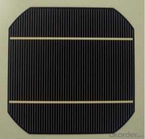
MONO5'(125*125mm)165
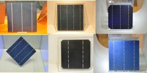
Monocrystalline silicon solar cell
Physical Characteristics
Dimension: 125mm×125mm±0.5mm
Diagonal: 165mm±0.5mm
Thickness(Si): 200±20 μm
Front(-) Back(+)
Blue anti-reflecting coating(silicon nitride); Aluminum back surface field;
1.6mmwide bus bars; 2.5mm wide soldering pads;
Distance between bus bars: 61mm . Distance between bus bars :61mm .
Electrical Characteristics
Efficiency(%) | 19.40 | 19.20 | 19.00 | 18.80 | 18.60 | 18.40 | 18.20 | 18.00 | 17.80 | 17.60 | 17.40 | 17.20 |
Pmpp(W) | 2.97 | 2.94 | 2.91 | 2.88 | 2.85 | 2.82 | 2.79 | 2.76 | 2.73 | 2.70 | 2.67 | 2.62 |
Umpp(V) | 0.537 | 0.535 | 0.533 | 0.531 | 0.527 | 0.524 | 0.521 | 0.518 | 0.516 | 0.515 | 0.513 | 0.509 |
Impp(A) | 5.531 | 5.495 | 5.460 | 5.424 | 5.408 | 5.382 | 5.355 | 5.328 | 5.291 | 5.243 | 5.195 | 4.147 |
Uoc(V) | 0.637 | 0.637 | 0.636 | 0.635 | 0.633 | 0.630 | 0.629 | 0.629 | 0.628 | 0.626 | 0.626 | 0.625 |
Isc(A) | 5.888 | 5.876 | 5.862 | 5.848 | 5.839 | 5.826 | 5.809 | 5.791 | 5.779 | 5.756 | 5.293 | 5.144 |
FAQ:
Q:How can i get some sample?
A:Yes , if you want order ,sample is not a problem.
Q:How about your solar panel efficency?
A: Our product efficency around 17.25%~18.25%.
Q:What’s the certificate you have got?
A: we have overall product certificate of ISO9001/ISO14001/CE/TUV/UL
- Q: What is the role of surface texturing on solar silicon wafers?
- The role of surface texturing on solar silicon wafers is to enhance light trapping and increase the absorption of photons.
- Q: Can solar silicon wafers be repaired?
- Yes, solar silicon wafers can be repaired to some extent. Minor damages like scratches and cracks can be repaired using various techniques such as polishing or filling with epoxy. However, significant damages or functional defects may require the replacement of the entire wafer. It is important to note that the repair process should be conducted by professionals to ensure the optimal performance and safety of the solar panel.
- Q: Can solar silicon wafers be used in concentrated photovoltaics (CPV)?
- Yes, solar silicon wafers can be used in concentrated photovoltaics (CPV). CPV systems use lenses or mirrors to concentrate sunlight onto a small area of solar cells, increasing their efficiency. Silicon wafers are commonly used in CPV systems as they are a reliable and efficient material for converting sunlight into electricity.
- Q: How are solar silicon wafers affected by potential-induced degradation?
- Solar silicon wafers are negatively affected by potential-induced degradation (PID). PID occurs when a high voltage potential is applied to the solar cells over an extended period, leading to a degradation in their performance. This degradation is primarily caused by the migration of sodium ions from the glass surface into the bulk silicon, resulting in the formation of a negative voltage bias between the p-n junction. This bias leads to an increased leakage current and a decrease in the power output of the solar cell. To mitigate the impact of PID, various techniques such as the use of anti-PID modules or the application of PID-resistant materials are employed in the manufacturing process of solar silicon wafers.
- Q: How do solar silicon wafers affect the overall flexibility of a solar panel?
- Solar silicon wafers do not directly affect the overall flexibility of a solar panel. The flexibility of a solar panel depends on the material and design of the panel itself, rather than the silicon wafers used in its construction. However, the thickness and type of silicon wafers can indirectly impact the flexibility by affecting the weight and rigidity of the panel.
- Q: What is the role of solar silicon wafers in reducing reliance on fossil fuels?
- Solar silicon wafers play a crucial role in reducing reliance on fossil fuels by serving as the foundation for solar cells, which convert sunlight into electricity. These wafers, made from purified silicon, are used to create the photovoltaic cells that make up solar panels. By harnessing the power of the sun, these panels generate clean and renewable energy, reducing the need for fossil fuel-based electricity production. As a result, solar silicon wafers enable the transition towards a more sustainable and environmentally friendly energy source, helping to combat climate change and decrease our dependence on finite fossil fuels.
- Q: How are solar silicon wafers affected by photon recycling?
- Solar silicon wafers are positively affected by photon recycling as it allows for more efficient use of photons. When photons are not absorbed by the first pass through the wafer, they have a chance to be reflected back and have another opportunity to be absorbed. This recycling process increases the overall absorption of photons, resulting in improved energy conversion efficiency of solar cells.
- Q: How are solar silicon wafers tested for mechanical strength and durability?
- Solar silicon wafers are tested for mechanical strength and durability through a series of rigorous tests. These tests typically involve subjecting the wafers to various mechanical stresses and environmental conditions to simulate real-world conditions. Some common tests include bend and flex tests, where the wafers are subjected to controlled bending forces, and impact tests, where they are exposed to physical impacts. Additionally, thermal cycling tests are performed to assess the wafers' ability to withstand extreme temperature changes. These tests help determine the structural integrity and durability of solar silicon wafers, ensuring their reliability and performance in solar cell applications.
- Q: How do solar silicon wafers contribute to job creation in the renewable energy sector?
- Solar silicon wafers contribute to job creation in the renewable energy sector by creating employment opportunities in various stages of the solar panel production process. The manufacturing of silicon wafers requires skilled workers in the semiconductor industry, leading to job creation in research and development, production, and quality control. Furthermore, as the demand for solar panels increases, more jobs are created in installation, maintenance, and operation of solar energy systems. This growth in the renewable energy sector not only supports existing jobs but also creates new opportunities for individuals seeking employment in a sustainable and rapidly expanding industry.
- Q: What is the impact of impurities on the performance of solar silicon wafers?
- The presence of impurities in solar silicon wafers can significantly impact their performance. Impurities can alter the electrical properties of the silicon, affecting the efficiency of the solar cell. For example, certain impurities can create energy barriers or recombination centers, reducing the overall conversion efficiency of the solar cell. Additionally, impurities can also lead to unwanted optical absorption, reducing the amount of light that can be absorbed and converted into electricity. Therefore, minimizing impurities and ensuring high-purity silicon wafers is crucial for maximizing the performance and efficiency of solar cells.
Send your message to us
Multicrystalline Silicon Solar Wafer - High Quality A Grade Poly/Monocrystalline 5V Solar Cell
- Loading Port:
- Shanghai
- Payment Terms:
- TT OR LC
- Min Order Qty:
- 1000 pc
- Supply Capability:
- 100000 pc/month
OKorder Service Pledge
OKorder Financial Service
Similar products
Hot products
Hot Searches
Related keywords
