


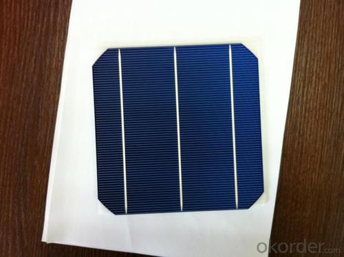

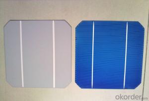
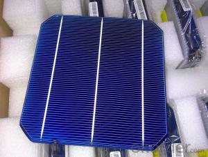
Mono Silicon Solar Wafer - 156mm*156mm Mono Solar Cells in Bulk Quantity Low Price Stock 18.0
- Ref Price:
-

- Loading Port:
- Shanghai
- Payment Terms:
- TT OR LC
- Min Order Qty:
- 1000 pc
- Supply Capability:
- 100000 pc/month
OKorder Service Pledge
OKorder Financial Service
You Might Also Like


Brief Introduction
- Up to 20.0% efficiency, one of the highest performing mono crystalline cells on the market
- Three bus bars boosts current collection over the entire cell area, leading to higher fill factors
- Blue anti-reflecting coating allows more sunlight be captured and converted to electricity
- Finer, closer fingers improves charge collections for improved energy yield
- Lower light-induced degradation leads to greater power output over the entire module lifetime
- All solar cells are tightly classified to optimize output of module
- Maximum yield and longevity due to hotspot prevention
- Premium appearance results in a highly uniform and aesthetically appealing module
Specification
- Product Mono-crystalline silicon solar cell
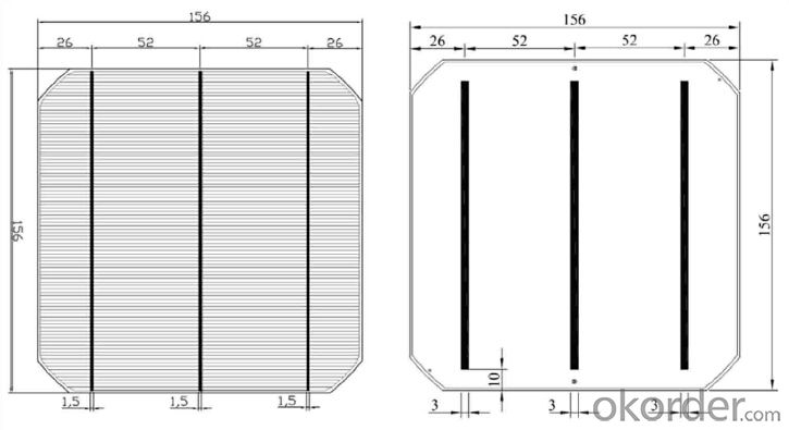
- Dimension 156 mm x 156 mm ± 0.5 mm
- Thickness 200 μm ± 30 μm
- Front 1.5 ± 0.1 mm busbar (silver)
- Silicon nitride antireflection coating
- Back 3.0 mm continuous soldering pads (silver)
- Back surface field (aluminum)
Electric performance parameters

- Testing conditions: 1000 W/m2, AM 1.5, 25 °C, Tolerance: Efficiency ± 0.2% abs., Pmpp ±1.5% rel.
- Imin : at 0.5 V
Light Intensity Dependence

Soldering Ability
- Peel Strength: > 1.0 N/mm (Pull soldered ribbon from busbar in 5 mm/s of 180°)
Dimension Figure

Quick Response
- Any time and anywhere, reply clients' email and solve all problems happen in the work at the first time.
- Remove clients doubts and offer the best solution at the first time.
- Give our clients the lastest news of the photovoltaic, update the newest stock informtion.
Production and Quality Control
- Precision cell efficiency sorting procedures
- Stringent criteria for color uniformity and appearance
- Reverse current and shunt resistance screening
- ISO9001,ISO14001 and OHSAS 18001,TUV Certificated


FAQ:
1. Q: Do you have your own factory?
A: Yes, we have. Our factory located in Jiangsu
2. Q: How can I visit your factory?
A: Before you visit,please contact us.We will show you the route or arrange a car to pick you up.
3. Q: Do you provide free sample?
A: Commenly we provide paid sample.
4. Q: Could you print our company LOGO on the nameplate and package?
A: Yes, we accept it.And need an Authorization Letter from you.
5. Q: Do you accept custom design on size?
A: Yes, if the size is reasonable.
6. Q: How can I be your agent in my country?
A: Please leave feedback. It's better for us to talk about details by email.
7. Q: Do you have solar project engineer who can guide me to install system?
A: Yes, we have a professional engineer team. They can teach you how to install a solar system.
- Q: How has the technology for solar silicon wafers evolved over time?
- The technology for solar silicon wafers has evolved significantly over time. Initially, the production of silicon wafers was a complex and expensive process, with low efficiency levels. However, advancements in manufacturing techniques and materials have led to the development of more efficient and cost-effective solar silicon wafers. These improvements include the introduction of thin-film solar cells, multicrystalline silicon wafers, and monocrystalline silicon wafers. Additionally, the size of the wafers has increased, allowing for larger solar cells and greater energy generation. Overall, the evolution of solar silicon wafer technology has resulted in increased efficiency, reduced costs, and widespread adoption of solar energy.
- Q: Can solar silicon wafers be used in solar-powered charging stations?
- Yes, solar silicon wafers can be used in solar-powered charging stations. These wafers are a key component in producing solar cells, which convert sunlight into electricity. Solar-powered charging stations utilize solar cells to capture sunlight and convert it into electrical energy to charge various devices. Therefore, solar silicon wafers play a crucial role in the functioning of solar-powered charging stations.
- Q: What is the typical production volume of solar silicon wafers?
- The typical production volume of solar silicon wafers can vary depending on the size and capacity of the manufacturing facility. However, large-scale production facilities are capable of producing millions to billions of solar silicon wafers annually to meet the growing demand for solar energy.
- Q: How is the efficiency of a solar silicon wafer measured?
- The efficiency of a solar silicon wafer is typically measured by calculating the percentage of sunlight that is converted into usable electricity. This is done by comparing the total power output of the solar cell to the amount of sunlight it receives. The higher the percentage, the more efficient the silicon wafer is at converting sunlight into electricity.
- Q: How to make monocrystalline silicon solar panels? Begged: specific steps
- Diffusion bondingSolar cells require a large area of PN junction to achieve the conversion of light energy to electrical energy, while the diffusion furnace is a special equipment for manufacturing solar cell PN junction. Tube type diffusion furnace is mainly composed of quartz boat download four parts part, gas chamber, a furnace body part and a holder part etc.. Generally, the liquid source of three phosphorus oxychloride is used as the diffusion source. The P type silicon wafer is placed in a quartz tube of a tube type diffusion furnace, and three nitrogen oxychloride is used in the quartz vessel at the temperature of 850---900 degrees Celsius, and the phosphorus atom is obtained through the reaction of the phosphorus oxychloride and the silicon wafer through the reaction of the phosphorus and the phosphorus. After a certain time, the phosphorus atom from the surrounding surface layer into a silicon wafer, and wafer to internal diffusion through the void between the silicon atoms, forming a N type semiconductor and P type semiconductor interface, namely PN junction. The PN junction made by this method has good uniformity, the uniformity of box resistance is less than ten percent, and the lifetime of less than 10ms. The manufacture of PN junction is the most basic and most important process in the production of solar cells. Because it is the formation of PN junction, so that the electrons and holes in the flow is no longer back to the original place, so that the formation of the current, using the wire will lead to the current, dc.
- Q: Can solar silicon wafers be used in hybrid solar systems?
- Yes, solar silicon wafers can be used in hybrid solar systems. Hybrid solar systems combine multiple renewable energy sources, such as solar and wind, to generate electricity. Solar silicon wafers are a key component of solar panels and can be integrated into hybrid systems to harness solar energy and contribute to the overall power generation.
- Q: Are there any environmental concerns associated with solar silicon wafers?
- Yes, there are some environmental concerns associated with solar silicon wafers. The production process of silicon wafers involves high energy consumption, which can contribute to carbon emissions if the energy comes from non-renewable sources. Additionally, the mining of raw materials like quartz and high-purity silicon can have negative impacts on ecosystems and local communities. However, it's important to note that compared to other energy sources, solar silicon wafers have significantly lower environmental impacts throughout their lifecycle, including reduced greenhouse gas emissions and water usage.
- Q: Can solar silicon wafers be used in water pumping systems?
- Yes, solar silicon wafers can be used in water pumping systems. Solar silicon wafers are commonly used in photovoltaic (PV) cells to convert sunlight into electricity. This electricity can power the water pumping systems, making them more sustainable and environmentally friendly.
- Q: How are solar silicon wafers affected by light-induced annealing?
- Light-induced annealing refers to the process where solar silicon wafers are exposed to intense light, causing the defects and impurities within the material to recombine and heal. This phenomenon improves the overall quality and efficiency of the wafers, making them more effective in converting sunlight into electricity.
- Q: Hello, the last time you gave me the answer on the silicon chip let me learn a lot, I would like to ask here, sapphire crystal density you know?
- Mineral name: corundum.Hard brittle materialChemical composition: Al 2 O 3; can contain Fe, Ti, Cr, V, Mn and other elements.Crystalline state.Crystal system: three party system;
Send your message to us
Mono Silicon Solar Wafer - 156mm*156mm Mono Solar Cells in Bulk Quantity Low Price Stock 18.0
- Ref Price:
-
- Loading Port:
- Shanghai
- Payment Terms:
- TT OR LC
- Min Order Qty:
- 1000 pc
- Supply Capability:
- 100000 pc/month
OKorder Service Pledge
OKorder Financial Service
Similar products


Hot products


Hot Searches
Related keywords

