


High Current Monocrystalline Solar Silicon Wafer 17.6% Polycrystalline Silicon Solar Cell Price
- Ref Price:
-

- Loading Port:
- Shanghai
- Payment Terms:
- TT OR LC
- Min Order Qty:
- 1000 pc
- Supply Capability:
- 100000 pc/month
OKorder Service Pledge
OKorder Financial Service
You Might Also Like


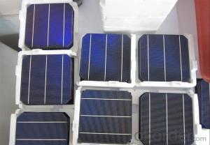
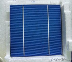
4 Bus Bars 156*156 17.6% efficiency poly solar cell
PHYSICAL CHARACTERISTICS
Dimension: 156mm x 156mm ± 0.5mm
Wafer Thickeness: 180um+20um and 200um+20um
Front(-) Four 1.2mm silver busbar
Silicon nitride blue anti-reflection coating
Back(+) aluminum back surface field
1.75mm(silver) wide segment soldering pads

Typical Electrical Characteristics
Efficiency | W(Pmpp) | V(Umpp) | A(Impp) | V(Uoc) | A(Isc) |
17.4-17.5 | 4.234 | 0.517 | 8.231 | 0.622 | 8.759 |
17.5-17.6 | 4.259 | 0.519 | 8.243 | 0.623 | 8.769 |
17.7-17.8 | 4.283 | 0.521 | 8.256 | 0.625 | 8.779 |
17.8-17.9 | 4.307 | 0.523 | 8.268 | 0.626 | 8.788 |
17.9-18.0 | 4.332 | 0.525 | 8.281 | 0.627 | 8.798 |
18.0-18.1 | 4.380 | 0.529 | 8.306 | 0.629 | 8.808 |
18.1-18.2 | 4.405 | 0.531 | 8.318 | 0.632 | 8.818 |
18.2-18.3 | 4.429 | 0.533 | 8.331 | 0.633 | 8.837 |
18.3-18.4 | 4.453 | 0.535 | 8.344 | 0.634 | 8.847 |
18.4-18.5 | 4.478 | 0.537 | 8.356 | 0.636 | 8.856 |
18.5-18.6 | 4.502 | 0.539 | 8.369 | 0.637 | 8.866 |
Efficiency | W(Pmpp) | V(Umpp) | A(Impp) | V(Uoc) | A(Isc) |
20.90-21.00 | 5.06 | 0.557 | 9.007 | 0.653 | 9.688 |
20.80-20.90 | 5.04 | 0.556 | 9.062 | 0.652 | 9.683 |
20.70-20.80 | 5.02 | 0.554 | 9.055 | 0.651 | 9.684 |
20.60-20.70 | 4.99 | 0.552 | 9.033 | 0.651 | 9.672 |
20.50-20.60 | 4.97 | 0.550 | 9.002 | 0.650 | 9.673 |
20.40-20.50 | 4.94 | 0.548 | 9.012 | 0.649 | 9.674 |
20.30-20.40 | 4.92 | 0.546 | 9.009 | 0.649 | 9.655 |
20.20-20.30 | 4.89 | 0.543 | 9.012 | 0.648 | 9.634 |
20.10-20.20 | 4.87 | 0.541 | 8.998 | 0.648 | 9.617 |
20.00-20.10 | 4.85 | 0.540 | 8.977 | 0.647 | 9.600 |
*Data under standard testing conditional (STC):1,000w/m2,AM1.5, 25°C , Pmax:Positive power tolerance.
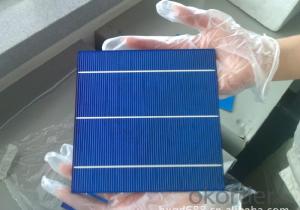
3 Bus Bars 156*156 17.4% efficiency poly solar cell
Dimension: 156 mm x 156 mm ± 0.5 mm
Wafer Thickeness: 156 mm x 156 mm ± 0.5 mm

Typical Electrical Characteristics:
| Efficiency code | 1660 | 1680 | 1700 | 1720 | 1740 | 1760 | 1780 | 1800 | 1820 | 1840 | 1860 |
| Efficiency (%) | 16.6 | 16.8 | 17.0 | 17.2 | 17.4 | 17.6 | 17.8 | 18.0 | 18.2 | 18.4 | 18.6 |
| Pmax (W) | 4.04 | 4.09 | 4.14 | 4.19 | 4.23 | 4.28 | 4.33 | 4.38 | 4.43 | 4.48 | 4.53 |
| Voc (V) | 0.612 | 0.615 | 0.618 | 0.621 | 0.624 | 0.627 | 0.629 | 0.63 | 0.633 | 0.635 | 0.637 |
| Isc (A) | 8.42 | 8.46 | 8.51 | 8.56 | 8.61 | 8.65 | 8.69 | 8.73 | 8.77 | 8.81 | 8.84 |
| Imp (A) | 7.91 | 7.99 | 8.08 | 8.16 | 8.22 | 8.27 | 8.33 | 8.38 | 8.43 | 8.48 | 8.53 |
* Testing conditions: 1000 W/m2, AM 1.5, 25 °C, Tolerance: Efficiency ± 0.2% abs., Pmpp ±1.5% rel.
* Imin : at 0.5 V
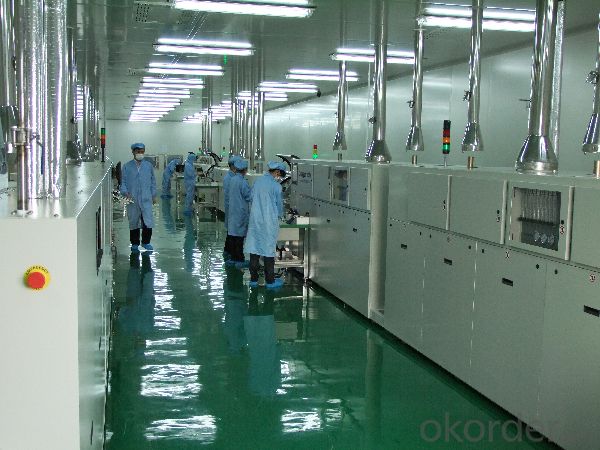
Production:

Package:

FAQ:
1. Q: Do you have your own factory?
A: Yes, we have. Our factory located in Jiangsu
2. Q: How can I visit your factory?
A: Before you visit,please contact us.We will show you the route or arrange a car to pick you up.
3. Q: Do you provide free sample?
A: Commenly we provide paid sample.
4. Q: Could you print our company LOGO on the nameplate and package?
A: Yes, we accept it.And need an Authorization Letter from you.
5. Q: Do you accept custom design on size?
A: Yes, if the size is reasonable.
6. Q: How can I be your agent in my country?
A: Please leave feedback. It's better for us to talk about details by email.
7. Q: Do you have solar project engineer who can guide me to install system?
A: Yes, we have a professional engineer team. They can teach you how to install a solar system.
- Q: Can solar silicon wafers be used in solar-powered remote sensing devices?
- Yes, solar silicon wafers can be used in solar-powered remote sensing devices. These wafers are commonly used in solar panels to convert sunlight into electrical energy, making them suitable for powering various remote sensing devices that require energy-efficient and sustainable power sources.
- Q: How do solar silicon wafers contribute to the overall efficiency of a solar panel?
- Solar silicon wafers are a crucial component of a solar panel as they play a significant role in enhancing its overall efficiency. These wafers are made from high-purity silicon, which allows them to absorb sunlight and convert it into electricity effectively. By providing a large surface area for light absorption, the silicon wafers increase the amount of sunlight that can be converted into electrical energy. Additionally, their unique crystalline structure ensures a high conversion efficiency, enabling more photons to be converted into electrons. Overall, solar silicon wafers significantly contribute to maximizing the power output and efficiency of solar panels.
- Q: What is the role of solar silicon wafers in reducing water consumption?
- Solar silicon wafers play a crucial role in reducing water consumption in the production of solar cells. Silicon wafers are the main component used in manufacturing solar cells, and their production requires significantly less water compared to other traditional energy sources such as fossil fuels. By transitioning to solar energy, which relies on silicon wafers, we can reduce the water-intensive processes associated with conventional energy generation, thereby conserving precious water resources.
- Q: How are solar silicon wafers protected from thermal shock during manufacturing?
- Solar silicon wafers are protected from thermal shock during manufacturing through several methods. One common approach is to use thermal annealing, where the wafers are gradually heated and cooled to relieve any internal stress and prevent cracking. Additionally, the use of specialized furnaces and controlled heating processes helps ensure a gradual and uniform temperature change, minimizing the risk of thermal shock. Finally, some manufacturers also apply protective coatings or use support materials to provide extra insulation and buffering against rapid temperature changes, further safeguarding the wafers from thermal shock.
- Q: How are solar silicon wafers connected within a solar panel?
- Solar silicon wafers are typically connected within a solar panel using a series of busbars and interconnect ribbons. The busbars, usually made of highly conductive materials like copper or silver, are placed on the front and back surfaces of the wafers to collect and transfer the generated electricity. These busbars are connected with interconnect ribbons, which are thin, flat metal strips that bridge the gaps between adjacent wafers. This interconnected network of wafers, busbars, and ribbons allows for the efficient flow of electricity, enabling the solar panel to convert sunlight into usable power.
- Q: How do solar silicon wafers contribute to reducing greenhouse gas emissions?
- Solar silicon wafers contribute to reducing greenhouse gas emissions by enabling the production of solar cells, which generate clean and renewable electricity. By harnessing sunlight to generate power, solar silicon wafers eliminate the need for fossil fuel-based energy sources, such as coal or natural gas power plants, which emit greenhouse gases like carbon dioxide and methane. Thus, the use of solar silicon wafers in solar cells helps mitigate climate change and reduce our overall carbon footprint.
- Q: Are solar silicon wafers affected by snow or ice accumulation?
- Yes, solar silicon wafers can be affected by snow or ice accumulation. Snow or ice covering the solar panels can reduce their efficiency by blocking sunlight from reaching the silicon wafers, which are responsible for converting solar energy into electricity. Additionally, the weight of accumulated snow or ice can put stress on the panels and potentially cause damage if they are not designed to withstand such loads. Regular cleaning or installing tilt systems can help mitigate the impact of snow or ice accumulation on solar silicon wafers.
- Q: What is the impact of light-induced degradation on the performance of solar silicon wafers?
- Light-induced degradation refers to the phenomenon where the performance of solar silicon wafers decreases over time due to exposure to sunlight. This degradation primarily affects the efficiency of the solar cells and reduces their power output. It occurs due to the formation of defects and impurities within the silicon material, which reduces the ability of the solar cells to convert sunlight into electricity. To mitigate this impact, manufacturers employ various techniques such as passivation layers or anti-reflective coatings to minimize light-induced degradation and ensure optimal performance of solar silicon wafers.
- Q: How is a degradation rate measured in a solar silicon wafer?
- The degradation rate in a solar silicon wafer is typically measured by assessing the decrease in the wafer's power output over a specific period of time, often expressed as a percentage per year. This measurement is obtained by comparing the initial power output of the wafer to its power output after a certain duration of usage or exposure to various environmental factors such as sunlight, temperature, and humidity. The degradation rate provides insight into the long-term reliability and performance of the wafer, allowing for effective monitoring and maintenance of solar photovoltaic systems.
- Q: Can solar silicon wafers be used in water desalination plants?
- Yes, solar silicon wafers can be used in water desalination plants. These wafers can be used to harness solar energy and convert it into electricity, which can then be utilized to power the desalination process. By using solar energy, desalination plants can become more sustainable and environmentally friendly.
Send your message to us
High Current Monocrystalline Solar Silicon Wafer 17.6% Polycrystalline Silicon Solar Cell Price
- Ref Price:
-
- Loading Port:
- Shanghai
- Payment Terms:
- TT OR LC
- Min Order Qty:
- 1000 pc
- Supply Capability:
- 100000 pc/month
OKorder Service Pledge
OKorder Financial Service
Similar products


Hot products


Hot Searches
Related keywords

