


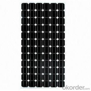
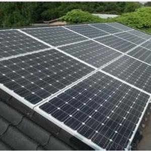
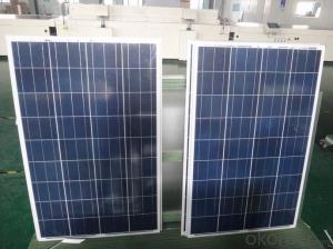
185W Solar Energy System Solar Panel with Monocrystalline Silicon Wafer Solar Cells
- Ref Price:
-

- Loading Port:
- China main port
- Payment Terms:
- TT OR LC
- Min Order Qty:
- 100 watt
- Supply Capability:
- 10000 watt/month
OKorder Service Pledge
OKorder Financial Service
You Might Also Like


185W Solar Energy System Solar Panel Monocrystalline Silicon Solar Cells
Main Characteristic
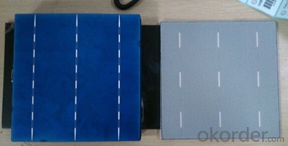
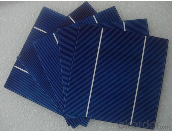
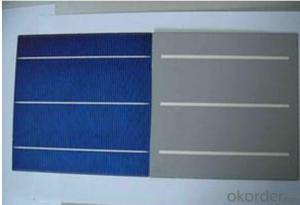
17.6%-18% High Efficiency A Grade 125mm Monocrystalline Solar Cells
1.First-class production technology and packaging technology.
2.Adopting the world's leading technology of silicon and polycrystalline silicon cells, power density, peak hours more battery power, higher conversion efficiency.
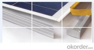
3.Beautiful, stable, easy to take down the anodic aluminum frame electric degrees and has a wind-resistant, anti-snow function.
Eff(%) | 18.00- 18.10 | 18.10- 18.20 | 18.20- 18.30 | 18.30- 18.40 | 18.40- 18.50 | 18.50- 18.60 | 18.60- 18.70 | 18.70- 18.80 | 18.80- 18.90 | 18.9- 19.0 | 19.1- 19.1 | 19.1- 19.2 |
Pm(W) | 4.30 | 4.33 | 4.35 | 4.37 | 4.40 | 4.42 | 4.44 | 4.47 | 4.49 | 4.52 | 4.54 | 4.56 |
Isc(A) | 8.71 | 8.73 | 8.76 | 8.77 | 8.78 | 8.82 | 8.83 | 8.85 | 8.86 | 8.88 | 8.9 | 8.93 |
Im(A) | 8.19 | 8.21 | 8.24 | 8.26 | 8.30 | 8.33 | 8.35 | 8.39 | 8.42 | 8.45 | 8.47 | 8.51 |
Voc(V) | 0.630 | 0.631 | 0.632 | 0.633 | 0.634 | 0.634 | 0.635 | 0.636 | 0.637 | 0.637 | 0.638 | 0.64 |
Vm(V) | 0.527 | 0.528 | 0.529 | 0.531 | 0.531 | 0.532 | 0.534 | 0.534 | 0.535 | 0.536 | 0.537 | 0.538 |
FF(%) | 78.6 | 78.7 | 78.8 | 79.0 | 79.2 | 79.3 | 79.5 | 79.6 | 79.8 | 80 | 80 | 80 |
Product Show


Shipping
1. Shipment shall be made only after PAYMENT is received.
2. Please do inform us your DETAILED ADDRESS AND CONTACT INFOMATION before shipment.
3. Shipment shall be made in THREE WORKING DAYS.
- Q: What is the role of a bypass diode in a solar silicon wafer?
- The role of a bypass diode in a solar silicon wafer is to provide an alternative current path when a portion of the wafer is shaded or damaged. It helps prevent power losses by bypassing the shaded or damaged section, allowing the unaffected sections to continue generating electricity efficiently.
- Q: What are the different manufacturing processes for solar silicon wafers?
- The different manufacturing processes for solar silicon wafers include crystallization, wafering, texturization, doping, passivation, and metallization.
- Q: What is the purpose of a conversion efficiency in a solar silicon wafer?
- The purpose of a conversion efficiency in a solar silicon wafer is to measure the effectiveness of the wafer in converting sunlight into usable electricity. It indicates how efficiently the wafer can capture and convert solar energy into electrical energy, thus determining the overall performance and potential of the solar panel or system. A higher conversion efficiency implies that the wafer can generate more electricity from the same amount of sunlight, making it more efficient and cost-effective in harnessing solar power.
- Q: What are the main defects in solar silicon wafers?
- The main defects in solar silicon wafers can include impurities, such as iron or boron, which can reduce the efficiency of the solar cells. Other defects may include cracks, dislocations, or grain boundaries, which can affect the structural integrity and electrical performance of the wafers.
- Q: What are the different types of solar silicon wafers available?
- The different types of solar silicon wafers available include monocrystalline, polycrystalline, and thin-film. Monocrystalline wafers are made from a single crystal structure, making them highly efficient but more expensive. Polycrystalline wafers are made from multiple crystal structures and are slightly less efficient but more affordable. Thin-film wafers are made by depositing a thin layer of silicon on a substrate and offer flexibility and lower production costs, but they have lower efficiency compared to crystalline wafers.
- Q: Can solar silicon wafers be used in thin-film solar cell technology?
- No, solar silicon wafers cannot be used in thin-film solar cell technology. Thin-film solar cells use different materials, such as amorphous silicon, cadmium telluride, or copper indium gallium selenide, to capture sunlight and convert it into electricity.
- Q: How are solar silicon wafers integrated into the electrical grid?
- Solar silicon wafers, which are the key component of solar panels, are integrated into the electrical grid through a series of steps. First, the solar panels made from silicon wafers are installed on rooftops, open spaces, or solar farms where they can capture sunlight. The panels convert sunlight into direct current (DC) electricity. To integrate this DC electricity into the electrical grid, an inverter is used to convert the DC electricity into alternating current (AC) electricity, which is the form of electricity used in the grid. The AC electricity produced by the solar panels is then connected to the electrical grid through a bi-directional meter. This meter measures the electricity produced by the solar panels and any excess electricity generated can be fed back into the grid, earning credits or reducing the energy bill of the owner. This integration allows the solar energy to be directly used by consumers or distributed to the wider electrical grid, contributing to the overall energy supply.
- Q: How is a conversion efficiency measured in a solar silicon wafer?
- Conversion efficiency in a solar silicon wafer is typically measured by calculating the ratio of the electrical power output from the solar cell to the total solar power input. This is done by taking into account factors such as the amount of sunlight absorbed, the electrical losses within the cell, and any other losses in the system. The resulting percentage is an indicator of how effectively the solar wafer is converting sunlight into usable electrical energy.
- Q: What is the typical lead time for ordering solar silicon wafers?
- The typical lead time for ordering solar silicon wafers can vary depending on several factors, including the supplier, quantity, and demand. However, it is common for lead times to range from a few weeks to a few months.
- Q: What is the effect of surface roughness on solar silicon wafers?
- The effect of surface roughness on solar silicon wafers is twofold. Firstly, a rough surface can enhance light trapping, increasing the chances of photon absorption and improving the overall efficiency of the solar cell. Secondly, it can also increase the surface recombination rate of charge carriers, leading to decreased performance. Therefore, a balance must be struck to optimize the surface roughness for maximum solar cell efficiency.
Send your message to us
185W Solar Energy System Solar Panel with Monocrystalline Silicon Wafer Solar Cells
- Ref Price:
-
- Loading Port:
- China main port
- Payment Terms:
- TT OR LC
- Min Order Qty:
- 100 watt
- Supply Capability:
- 10000 watt/month
OKorder Service Pledge
OKorder Financial Service
Similar products

Hot products


Hot Searches
Related keywords

