


Solar Silicon Wafer Mono Solar Cells 156mm*156mm in Bulk Quantity Low Price Stock 18.4
- Ref Price:
-

- Loading Port:
- Shanghai
- Payment Terms:
- TT OR LC
- Min Order Qty:
- 1000 pc
- Supply Capability:
- 100000 pc/month
OKorder Service Pledge
OKorder Financial Service
You Might Also Like


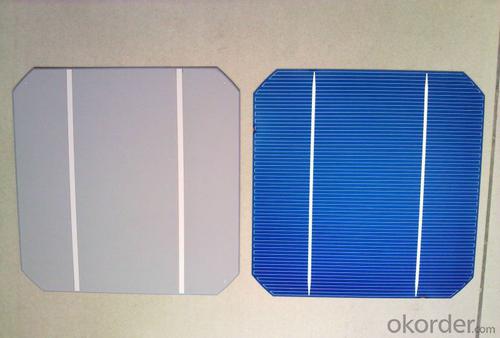
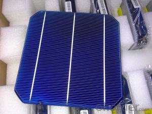
Brief Introduction
- Up to 20.0% efficiency, one of the highest performing mono crystalline cells on the market
- Three bus bars boosts current collection over the entire cell area, leading to higher fill factors
- Blue anti-reflecting coating allows more sunlight be captured and converted to electricity
- Finer, closer fingers improves charge collections for improved energy yield
- Lower light-induced degradation leads to greater power output over the entire module lifetime
- All solar cells are tightly classified to optimize output of module
- Maximum yield and longevity due to hotspot prevention
- Premium appearance results in a highly uniform and aesthetically appealing module
Specification
- Product Mono-crystalline silicon solar cell
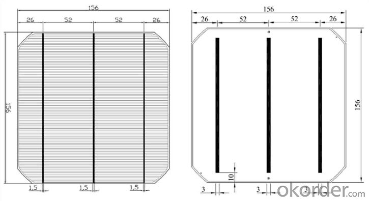
- Dimension 156 mm x 156 mm ± 0.5 mm
- Thickness 200 μm ± 30 μm
- Front 1.5 ± 0.1 mm busbar (silver)
- Silicon nitride antireflection coating
- Back 3.0 mm continuous soldering pads (silver)
- Back surface field (aluminum)
Electric performance parameters

- Testing conditions: 1000 W/m2, AM 1.5, 25 °C, Tolerance: Efficiency ± 0.2% abs., Pmpp ±1.5% rel.
- Imin : at 0.5 V
Light Intensity Dependence

Soldering Ability
- Peel Strength: > 1.0 N/mm (Pull soldered ribbon from busbar in 5 mm/s of 180°)
Dimension Figure

Quick Response
- Any time and anywhere, reply clients' email and solve all problems happen in the work at the first time.
- Remove clients doubts and offer the best solution at the first time.
- Give our clients the lastest news of the photovoltaic, update the newest stock informtion.
Production and Quality Control
- Precision cell efficiency sorting procedures
- Stringent criteria for color uniformity and appearance
- Reverse current and shunt resistance screening
- ISO9001,ISO14001 and OHSAS 18001,TUV Certificated


FAQ:
1. Q: Do you have your own factory?
A: Yes, we have. Our factory located in Jiangsu
2. Q: How can I visit your factory?
A: Before you visit,please contact us.We will show you the route or arrange a car to pick you up.
3. Q: Do you provide free sample?
A: Commenly we provide paid sample.
4. Q: Could you print our company LOGO on the nameplate and package?
A: Yes, we accept it.And need an Authorization Letter from you.
5. Q: Do you accept custom design on size?
A: Yes, if the size is reasonable.
6. Q: How can I be your agent in my country?
A: Please leave feedback. It's better for us to talk about details by email.
7. Q: Do you have solar project engineer who can guide me to install system?
A: Yes, we have a professional engineer team. They can teach you how to install a solar system.
- Q: What is the role of surface texturing on solar silicon wafers?
- The role of surface texturing on solar silicon wafers is to enhance light trapping and increase the absorption of photons.
- Q: How do solar silicon wafers perform in cold climates?
- Solar silicon wafers perform well in cold climates as the low temperatures actually enhance their efficiency. The cold weather helps to reduce the resistance in the solar cells, allowing them to produce more electricity. However, extreme cold can lead to issues such as snow accumulation, which may temporarily hinder their performance until cleared. Overall, solar silicon wafers are designed to withstand and operate efficiently in cold weather conditions.
- Q: What is the purpose of texturing the surface of a solar silicon wafer?
- The purpose of texturing the surface of a solar silicon wafer is to increase its light absorption capacity. By introducing microscopic structures or patterns on the wafer's surface, the texture helps to scatter and trap light, allowing for better interaction with the silicon material and enhancing the overall efficiency of the solar cell.
- Q: Can solar silicon wafers be reused or repurposed after their lifespan in a solar panel?
- Yes, solar silicon wafers can be reused or repurposed after their lifespan in a solar panel. While they may no longer be suitable for generating electricity in solar panels, these wafers can be recycled to extract valuable materials such as silicon, silver, and glass. The extracted materials can then be used in various industries, including electronics, semiconductors, and glass manufacturing, promoting a more sustainable approach to resource utilization.
- Q: Are there any initiatives to improve the sustainability of solar silicon wafers?
- Yes, there are several initiatives aimed at improving the sustainability of solar silicon wafers. These initiatives focus on reducing the environmental impact of wafer production by optimizing manufacturing processes, increasing the use of recycled materials, and exploring alternative materials that are more sustainable. Additionally, efforts are being made to improve the efficiency of solar cells, reducing the amount of silicon needed per wafer and minimizing waste. These initiatives aim to make solar silicon wafer production more environmentally friendly and economically viable in the long term.
- Q: Can solar silicon wafers be used in smart grid systems?
- Yes, solar silicon wafers can be used in smart grid systems. Solar silicon wafers are the key component in solar panels, which generate electricity from sunlight. When integrated with smart grid systems, solar panels using silicon wafers can help supply clean and sustainable energy to the grid, contributing to the overall energy management and efficiency of the smart grid system.
- Q: How do solar silicon wafers contribute to reducing dependence on fossil fuels?
- Solar silicon wafers contribute to reducing dependence on fossil fuels by converting sunlight into electricity through the photovoltaic effect. These wafers are the key component in solar panels, which generate clean and renewable energy. By harnessing solar power, we can reduce the need for fossil fuel-based electricity generation, consequently reducing greenhouse gas emissions and environmental degradation associated with traditional energy sources.
- Q: What are the different manufacturing methods for solar silicon wafers?
- There are primarily three manufacturing methods for solar silicon wafers: the Czochralski (CZ) method, the Float Zone (FZ) method, and the Multi-Crystalline Silicon (mc-Si) method. The CZ method involves melting high-purity silicon in a crucible and slowly pulling a single crystal from the molten material. The FZ method also melts silicon, but instead of pulling a single crystal, a small seed crystal is dipped into the molten material and then slowly moved upwards, allowing a single crystal to form. The mc-Si method utilizes multiple silicon crystals, which are melted and then casted into blocks, which are later sliced into wafers. Each method has its own advantages and disadvantages, impacting the cost, quality, and efficiency of the resulting solar silicon wafers.
- Q: What is the role of solar silicon wafers in reducing the digital divide?
- Solar silicon wafers play a crucial role in reducing the digital divide by enabling the production of affordable solar panels. These solar panels can be used to generate clean and sustainable electricity, providing access to energy in remote and underprivileged areas. This access to electricity is essential for powering electronic devices and bridging the digital divide by connecting people to the internet and other digital tools. Additionally, solar silicon wafers contribute to the development of renewable energy infrastructure, which can boost economic growth and create employment opportunities, further helping to reduce the digital divide.
- Q: How is a solar silicon wafer connected to other components in a solar panel?
- A solar silicon wafer is typically connected to other components in a solar panel through a series of electrical connections. These connections are made using conductive materials, such as metal ribbons or wires, which are soldered to the front and back contacts of the wafer. The ribbons or wires are then connected to the junction box of the solar panel, allowing for the transfer of electrical current generated by the wafer to other components, such as the inverter or battery, for further use or storage.
Send your message to us
Solar Silicon Wafer Mono Solar Cells 156mm*156mm in Bulk Quantity Low Price Stock 18.4
- Ref Price:
-
- Loading Port:
- Shanghai
- Payment Terms:
- TT OR LC
- Min Order Qty:
- 1000 pc
- Supply Capability:
- 100000 pc/month
OKorder Service Pledge
OKorder Financial Service
Similar products


Hot products


Hot Searches
Related keywords

