


Solar Silicon Wafer for Sale - High Quality A Grade Polycrystalline 5V 16.8% Solar Cell
- Ref Price:
-

- Loading Port:
- Shanghai
- Payment Terms:
- TT OR LC
- Min Order Qty:
- 1000 pc
- Supply Capability:
- 100000 pc/month
OKorder Service Pledge
OKorder Financial Service
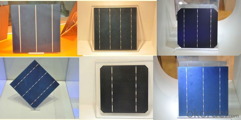
You Might Also Like


Specifications
hot sale solar cell
1.16.8%~18.25% high efficiency
2.100% checked quality
3.ISO9001/ISO14001/TUV/CE/UL
4.stable performance
We can offer you the best quality products and services, don't miss !
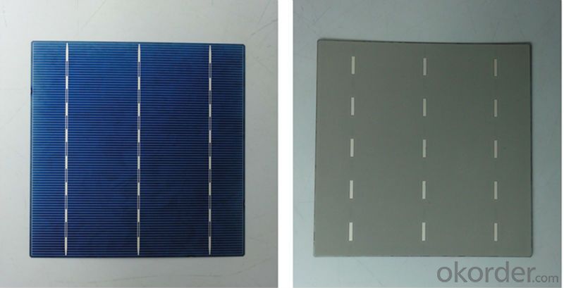
POLY6'(156*156)
Polycrystalline Silicon Solar cell
Physical Characteristics
Dimension: 156mm×156mm±0.5mm
Diagonal: 220mm±0.5mm
Thickness(Si): 200±20 μm
Front(-) Back(+)
Blue anti-reflecting coating (silicon nitride); Aluminum back surface field;
1.5mm wide bus bars; 2.0mm wide soldering pads;
Distance between bus bars: 51mm . Distance between bus bars :51mm .
Electrical Characteristics
Efficiency(%) | 18.00 | 17.80 | 17.60 | 17.40 | 17.20 | 16.80 | 16.60 | 16.40 | 16.20 | 16.00 | 15.80 | 15.60 |
Pmpp(W) | 4.33 | 4.29 | 4.24 | 4.19 | 4.14 | 4.09 | 4.04 | 3.99 | 3.94 | 3.90 | 3.86 | 3.82 |
Umpp(V) | 0.530 | 0.527 | 0.524 | 0.521 | 0.518 | 0.516 | 0.514 | 0.511 | 0.509 | 0.506 | 0.503 | 0.501 |
Impp(A) | 8.159 | 8.126 | 8.081 | 8.035 | 7.990 | 7.938 | 7.876 | 7.813 | 7.754 | 7.698 | 7.642 | 7.586 |
Uoc(V) | 0.633 | 0.631 | 0.628 | 0.625 | 0.623 | 0.620 | 0.618 | 0.617 | 0.615 | 0.613 | 0.611 | 0.609 |
Isc(A) | 8.709 | 8.677 | 8.629 | 8.578 | 8.531 | 8.478 | 8.419 | 8.356 | 8.289 | 8.220 | 8.151 | 8.083 |

MONO5'(125*125mm)165
Monocrystalline silicon solar cell
Physical Characteristics
Dimension: 125mm×125mm±0.5mm
Diagonal: 165mm±0.5mm
Thickness(Si): 200±20 μm
Front(-) Back(+)
Blue anti-reflecting coating(silicon nitride); Aluminum back surface field;
1.6mmwide bus bars; 2.5mm wide soldering pads;
Distance between bus bars: 61mm . Distance between bus bars :61mm .
Electrical Characteristics
Efficiency(%) | 19.40 | 19.20 | 19.00 | 18.80 | 18.60 | 18.40 | 18.20 | 18.00 | 17.80 | 17.60 | 17.40 | 17.20 |
Pmpp(W) | 2.97 | 2.94 | 2.91 | 2.88 | 2.85 | 2.82 | 2.79 | 2.76 | 2.73 | 2.70 | 2.67 | 2.62 |
Umpp(V) | 0.537 | 0.535 | 0.533 | 0.531 | 0.527 | 0.524 | 0.521 | 0.518 | 0.516 | 0.515 | 0.513 | 0.509 |
Impp(A) | 5.531 | 5.495 | 5.460 | 5.424 | 5.408 | 5.382 | 5.355 | 5.328 | 5.291 | 5.243 | 5.195 | 4.147 |
Uoc(V) | 0.637 | 0.637 | 0.636 | 0.635 | 0.633 | 0.630 | 0.629 | 0.629 | 0.628 | 0.626 | 0.626 | 0.625 |
Isc(A) | 5.888 | 5.876 | 5.862 | 5.848 | 5.839 | 5.826 | 5.809 | 5.791 | 5.779 | 5.756 | 5.293 | 5.144 |

FAQ:
Q:How can i get some sample?
A:Yes , if you want order ,sample is not a problem.
Q:How about your solar panel efficency?
A: Our product efficency around 17.25%~18.25%.
Q:What’s the certificate you have got?
A: we have overall product certificate of ISO9001/ISO14001/CE/TUV/UL
- Q: What is the role of back contacts on solar silicon wafers?
- The role of back contacts on solar silicon wafers is to provide an electrical connection for the flow of current generated by the solar cells. They are typically made of metal and are placed on the backside of the wafer, opposite to the side exposed to sunlight. Back contacts help in collecting and conducting the electricity produced by the solar cells to the external circuit, enabling the utilization of solar energy for various applications.
- Q: What is the role of back contact in solar silicon wafers?
- The role of back contact in solar silicon wafers is to provide electrical connection and support for the flow of current generated by the photovoltaic cells. It acts as a conductive layer that allows the captured solar energy to be efficiently transferred to external circuitry for use or storage. Additionally, it helps in maintaining the structural integrity of the wafer and protects the sensitive layers of the solar cell from external factors such as moisture and physical damage.
- Q: I would like to ask: silicon annealing treatment is how? Why anneal? Does annealing have an effect on the resistivity and the minority lifetime?
- Why anneal? One reason is that silicon contains oxygen, oxygen has the role of absorbing impurities. The oxygen near the surface of the silicon wafer can be removed from the surface during annealing, so as to reduce the number of impurities near the surface. Facilitates device fabrication;Annealing has a certain influence on the resistivity and minority lifetime.For reference.
- Q: What is the role of a junction box connector in a solar silicon wafer?
- The role of a junction box connector in a solar silicon wafer is to provide a secure and reliable connection between the solar cells on the wafer and the external electrical system. It allows for the efficient transfer of electrical current generated by the solar cells to the circuitry and wiring of a solar panel. Additionally, the junction box connector helps protect the electrical connections from environmental factors such as moisture, dust, and temperature fluctuations, ensuring the longevity and performance of the solar panel.
- Q: Are there any ongoing research efforts to enhance the efficiency of solar silicon wafers?
- Yes, there are ongoing research efforts to enhance the efficiency of solar silicon wafers. Researchers are working on various approaches such as developing new materials and technologies to increase light absorption, reducing energy losses due to recombination, improving surface passivation, and exploring novel cell architectures. These efforts aim to increase the conversion efficiency of solar silicon wafers, ultimately leading to more cost-effective and efficient solar panels.
- Q: How are solar silicon wafers affected by light-induced annealing?
- Solar silicon wafers are positively affected by light-induced annealing. This process helps to reduce defects and improve the overall efficiency of the wafers by repairing crystal lattice damage caused during fabrication.
- Q: The significance of silicon wafer heat treatment
- Heat treatment at 650 DEG C, under the condition of rapid cooling (that is, rapidly over the temperature of 450 DEG C), the thermal donor can be eliminated. That is, we can observe that the resistivity of N sample is high, and the resistivity of P sample is low.Precipitation: 800-1200 DEG C, on behalf of temperature 1050 degrees CHeat treatment at 1050 DEG C, will bring oxygen precipitation, and the formation of defects caused by precipitation defects.Restore: > 1200
- Q: Can solar silicon wafers be used in underwater solar energy systems?
- Yes, solar silicon wafers can be used in underwater solar energy systems. However, special considerations need to be taken into account to ensure their effectiveness and longevity in underwater environments.
- Q: How do solar silicon wafers handle extreme temperatures?
- Solar silicon wafers are designed to handle extreme temperatures quite well. They are typically made from high-grade silicon materials that can withstand both very high and low temperatures. The silicon material has a high melting point and excellent thermal stability, allowing it to handle the heat generated from sunlight and the surrounding environment. Additionally, solar cells are often encapsulated with protective layers and materials that provide further insulation and temperature resistance. This ensures that solar silicon wafers can continue to generate electricity efficiently, even in extreme temperature conditions.
- Q: What is the role of solar silicon wafers in promoting energy independence at the community level?
- Solar silicon wafers play a crucial role in promoting energy independence at the community level by serving as the key component in solar photovoltaic (PV) panels. These wafers are responsible for converting sunlight into electricity, enabling communities to generate their own clean and renewable energy. By harnessing solar power, communities can reduce their dependence on traditional fossil fuel sources, contribute to a greener environment, and potentially save on energy costs. Solar silicon wafers are instrumental in empowering communities to take control of their energy needs and contribute towards a more sustainable future.
Send your message to us
Solar Silicon Wafer for Sale - High Quality A Grade Polycrystalline 5V 16.8% Solar Cell
- Ref Price:
-
- Loading Port:
- Shanghai
- Payment Terms:
- TT OR LC
- Min Order Qty:
- 1000 pc
- Supply Capability:
- 100000 pc/month
OKorder Service Pledge
OKorder Financial Service
Similar products


Hot products


Hot Searches
Related keywords

