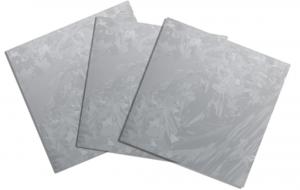

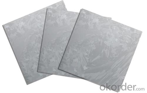

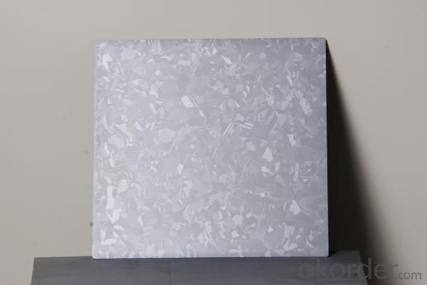
Silicon Wafer in Solar Photovoltaic Cells - Polycrystalline/Multiple Solar Silicon Wafer 156*156
- Ref Price:
-

- Loading Port:
- Shanghai Port
- Payment Terms:
- TT or LC
- Min Order Qty:
- 100 Pieces PCS
- Supply Capability:
- 700MW/Per Year PCS/month
OKorder Service Pledge
Quality Product, Order Online Tracking, Timely Delivery
OKorder Financial Service
Credit Rating, Credit Services, Credit Purchasing
You Might Also Like


Specifications of Polycrystalline Silicon Wafer
Format : 156 mm × 156 mm ± 0.5 mm
Thickness : 200μm ± 10 μm
| Product name | Poly Wafer |
| Conductive type | P Type |
| Square size wafer (mm) | 156×156±0.5 |
| 219.20±0.5 | |
| Corner (mm)
|
1±0.5、45°±10º |
| 200±20 | |
| Total thickness(um) | ≤40 |
| Resistivity ranges(Ωcm) | 1-3 |
| Doping elements | boron |
| Carbon content(atoms/cc) | ≤8*1017 |
| Oxygen content(atoms/cc) | ≤1*1018 |
| Lifetime(μs) | ≥2 |
| Surface quality | No crack, gap, missing Angle, perforated, window, microcrystalline |
| Warping degrees(μm) | ≤50 |
| Neighbouring vertical degree | 90±0.5° |
| Side damage(mm) | ≤0.5mm(length)×0.3mm(width),(not more than 2 per wafer) |
| Line mark(μm) | ≤15 |
Usage and Applications of Poly Wafers
Poly Solar Wafers mainly used in Poly Solar Cells, with high efficiency and reliable quality. Our Wafer can promise the 25 years life span and have passed PID test.
Packaging & Delivery of Poly Wafers
Carton Box Package and Deliver by air
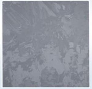
Factory Picture of Poly Wafers

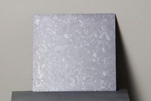
Package Picture of Poly Wafers

- Q: Can solar silicon wafers be used in off-grid applications?
- Yes, solar silicon wafers can be used in off-grid applications. Solar panels made from silicon wafers are commonly used to generate electricity in off-grid locations where there is no access to the power grid. These panels capture sunlight and convert it into electricity, which can then be used to power various off-grid applications such as remote cabins, boats, and RVs.
- Q: What is the role of solar silicon wafers in reducing water consumption?
- Solar silicon wafers play a crucial role in reducing water consumption by enabling the production of solar panels, which generate electricity without the need for water-intensive cooling systems. This helps alleviate the strain on water resources, as traditional power generation methods often require substantial amounts of water for cooling purposes.
- Q: What are the different wafer orientations used in solar silicon wafer production?
- There are primarily three different wafer orientations used in solar silicon wafer production: the (100) orientation, the (111) orientation, and the (110) orientation. Each orientation has its own advantages and characteristics, which are considered during the manufacturing process to optimize the efficiency and performance of solar panels.
- Q: Can solar silicon wafers be used in electric vehicle charging infrastructure?
- Yes, solar silicon wafers can be used in electric vehicle charging infrastructure. These wafers can be utilized to harness solar energy, which can then be converted to electricity and used to power electric vehicle charging stations. This approach promotes renewable energy usage and reduces dependence on traditional power sources, making it an environmentally friendly and sustainable option for electric vehicle charging infrastructure.
- Q: How does the efficiency of a solar silicon wafer change over time?
- The efficiency of a solar silicon wafer tends to decrease over time due to various factors such as degradation, wear and tear, and exposure to environmental conditions. These factors can lead to the accumulation of dirt, dust, and microcracks on the surface of the wafer, which hampers its ability to convert sunlight into electricity efficiently. Additionally, prolonged exposure to sunlight and heat can cause the wafer to degrade, resulting in a gradual reduction in its overall efficiency. Regular maintenance and cleaning can help mitigate these effects and prolong the lifespan of the solar silicon wafer.
- Q: How are solar silicon wafers protected from transportation damage?
- Solar silicon wafers are typically protected from transportation damage through various measures, such as packaging them in special containers or boxes that provide cushioning and shock absorption. These containers often include foam inserts or other materials that prevent the wafers from moving or vibrating during transit, minimizing the risk of breakage or cracking. Additionally, some manufacturers may use specialized handling procedures and equipment to ensure safe transportation of the wafers, reducing the potential for damage during loading, unloading, or movement.
- Q: How much is the thickness of the silicon wafer
- And two knives. We do DIP package, 4 inch wafer to thin to 0.300mm; 6 inch wafer to be reduced to about 0.320mm, error 0.020mm.
- Q: What are the main defects in solar silicon wafers?
- The main defects in solar silicon wafers include crystallographic defects such as dislocations, grain boundaries, and stacking faults. These defects can reduce the efficiency of solar cells by limiting the flow of electrons, causing recombination of charge carriers, and affecting the overall electrical properties of the wafers.
- Q: How do solar silicon wafers compare to other types of solar cell technologies?
- Solar silicon wafers, commonly used in crystalline silicon solar cells, have several advantages over other types of solar cell technologies. Firstly, they have high efficiency levels, with conversion rates reaching up to 25%. Additionally, silicon wafers are well-established and have a long track record of reliability and durability. They are also readily available and affordable due to mass production. However, silicon wafers require a significant amount of energy and resources during manufacturing. In contrast, other solar cell technologies like thin-film solar cells may have lower efficiency but offer flexibility, lighter weight, and lower manufacturing costs. Ultimately, the choice between solar silicon wafers and other technologies depends on specific requirements such as cost, efficiency, and application.
- Q: Can solar silicon wafers be made flexible for applications in wearable devices?
- Yes, solar silicon wafers can be made flexible for applications in wearable devices. Advances in technology have allowed for the development of flexible solar cells that use thin-film materials instead of rigid silicon wafers. These flexible solar cells can be integrated into wearable devices, such as smartwatches or clothing, allowing them to generate power from sunlight while maintaining their flexibility and functionality.
Our company is a world class resources and green energy developer, operator and supplier with its engagement in green energy development, integration and operation. We strives to offer highly efficient, eco-friendly, economical and reliable energy solutions through an integrated and diversified energy industrial chain. In adherence to the philosophy of bringing green power to life, the Group stays committed to continuously providing high-quality energy and services for a better living environment. Under approaches of people-oriented, excellence-foremost, value-creation and harmony-pursuant, our Group is determined to become a respected world-class green energy conglomerate.
1. Manufacturer Overview
| Location | |
| Year Established | |
| Annual Output Value | |
| Main Markets | |
| Company Certifications |
2. Manufacturer Certificates
| a) Certification Name | |
| Range | |
| Reference | |
| Validity Period |
3. Manufacturer Capability
| a) Trade Capacity | |
| Nearest Port | |
| Export Percentage | |
| No.of Employees in Trade Department | |
| Language Spoken: | |
| b) Factory Information | |
| Factory Size: | |
| No. of Production Lines | |
| Contract Manufacturing | |
| Product Price Range | |
Send your message to us
Silicon Wafer in Solar Photovoltaic Cells - Polycrystalline/Multiple Solar Silicon Wafer 156*156
- Ref Price:
-
- Loading Port:
- Shanghai Port
- Payment Terms:
- TT or LC
- Min Order Qty:
- 100 Pieces PCS
- Supply Capability:
- 700MW/Per Year PCS/month
OKorder Service Pledge
Quality Product, Order Online Tracking, Timely Delivery
OKorder Financial Service
Credit Rating, Credit Services, Credit Purchasing
Similar products


Hot products


Hot Searches

