


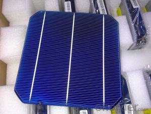
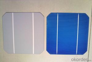
Monocrystalline Solar Grade Silicon Wafer - Mono Solar Cells 156mm*156mm in Bulk Quantity Low Price Stock 18.2
- Ref Price:
-

- Loading Port:
- Shanghai
- Payment Terms:
- TT OR LC
- Min Order Qty:
- 1000 pc
- Supply Capability:
- 100000 pc/month
OKorder Service Pledge
OKorder Financial Service
You Might Also Like


Brief Introduction
- Up to 20.0% efficiency, one of the highest performing mono crystalline cells on the market
- Three bus bars boosts current collection over the entire cell area, leading to higher fill factors
- Blue anti-reflecting coating allows more sunlight be captured and converted to electricity
- Finer, closer fingers improves charge collections for improved energy yield
- Lower light-induced degradation leads to greater power output over the entire module lifetime
- All solar cells are tightly classified to optimize output of module
- Maximum yield and longevity due to hotspot prevention
- Premium appearance results in a highly uniform and aesthetically appealing module
Specification
- Product Mono-crystalline silicon solar cell
- Dimension 156 mm x 156 mm ± 0.5 mm
- Thickness 200 μm ± 30 μm
- Front 1.5 ± 0.1 mm busbar (silver)
- Silicon nitride antireflection coating
- Back 3.0 mm continuous soldering pads (silver)
- Back surface field (aluminum)
Electric performance parameters

- Testing conditions: 1000 W/m2, AM 1.5, 25 °C, Tolerance: Efficiency ± 0.2% abs., Pmpp ±1.5% rel.
- Imin : at 0.5 V
Light Intensity Dependence

Soldering Ability
- Peel Strength: > 1.0 N/mm (Pull soldered ribbon from busbar in 5 mm/s of 180°)
Dimension Figure

Quick Response
- Any time and anywhere, reply clients' email and solve all problems happen in the work at the first time.
- Remove clients doubts and offer the best solution at the first time.
- Give our clients the lastest news of the photovoltaic, update the newest stock informtion.
Production and Quality Control
- Precision cell efficiency sorting procedures
- Stringent criteria for color uniformity and appearance
- Reverse current and shunt resistance screening
- ISO9001,ISO14001 and OHSAS 18001,TUV Certificated


FAQ:
1. Q: Do you have your own factory?
A: Yes, we have. Our factory located in Jiangsu
2. Q: How can I visit your factory?
A: Before you visit,please contact us.We will show you the route or arrange a car to pick you up.
3. Q: Do you provide free sample?
A: Commenly we provide paid sample.
4. Q: Could you print our company LOGO on the nameplate and package?
A: Yes, we accept it.And need an Authorization Letter from you.
5. Q: Do you accept custom design on size?
A: Yes, if the size is reasonable.
6. Q: How can I be your agent in my country?
A: Please leave feedback. It's better for us to talk about details by email.
7. Q: Do you have solar project engineer who can guide me to install system?
A: Yes, we have a professional engineer team. They can teach you how to install a solar system.
- Q: What is the role of surface passivation on solar silicon wafers?
- The role of surface passivation on solar silicon wafers is to improve the efficiency and performance of the solar cells. Passivation involves the application of a thin layer of material on the surface of the silicon wafer to reduce surface recombination, which is the loss of electrons and holes at the surface. This helps to minimize the loss of charge carriers and improves the overall electrical properties of the solar cell. By reducing surface recombination, surface passivation increases the conversion efficiency of the solar cell and enhances its ability to generate electricity from sunlight.
- Q: Can solar silicon wafers be used in solar-powered transportation systems?
- Yes, solar silicon wafers can be used in solar-powered transportation systems. They are commonly used in the production of solar panels, which can be installed on vehicles to harness solar energy and power the transportation systems.
- Q: How are defects in solar silicon wafers detected and minimized?
- Defects in solar silicon wafers are detected through various methods such as visual inspection, microscopy, and electrical testing. Visual inspection involves examining the surface of the wafers for any visible defects like cracks, scratches, or impurities. Microscopy techniques like scanning electron microscopy (SEM) are used to further analyze the wafers at a microscopic level, identifying any structural or material defects. Additionally, electrical testing is performed to evaluate the electrical properties of the wafers, ensuring they meet the required specifications. To minimize defects, manufacturers employ stringent quality control measures during the production process, use high-quality raw materials, and implement advanced purification techniques to purify the silicon.
- Q: How is the quality of a solar silicon wafer measured?
- The quality of a solar silicon wafer is typically measured through various tests and evaluations. These include monitoring the electrical properties such as resistivity and carrier lifetime, as well as assessing the physical characteristics like crystal structure, surface texture, and overall thickness uniformity. Additionally, optical measurements such as reflectivity and transmission are also taken into account. These evaluations help determine the efficiency and performance of the wafer in converting sunlight into electricity, ultimately indicating its quality.
- Q: Can solar silicon wafers be used in harsh environments?
- Yes, solar silicon wafers can be used in harsh environments. They are designed to withstand various environmental conditions such as extreme temperatures, high humidity, and exposure to UV radiation. The wafers are typically coated with protective materials to enhance their durability and resistance to corrosion, making them suitable for harsh outdoor environments.
- Q: How is a junction box integrated into a solar silicon wafer?
- A junction box is typically integrated into a solar silicon wafer by being attached to the backside of the wafer. The junction box houses the electrical connections and components necessary for the solar panel to function, such as diodes, bypass diodes, and connectors. It is securely sealed to protect the components from environmental factors and ensure reliable performance.
- Q: What is the role of surface texturing in solar silicon wafers?
- The role of surface texturing in solar silicon wafers is to increase the efficiency of solar cells by enhancing light trapping and reducing reflection.
- Q: How to make resistance on a piece of silicon chip (IC)? Read a lot of related articles, but also the first silicon oxidation, in the end is how? Best draw a
- You say SiO2 is equivalent to the boundary layer and layer.Wiring diagram... Tools are not enough brain.
- Q: What is the typical efficiency range of solar silicon wafers?
- The typical efficiency range of solar silicon wafers is between 15% to 22%.
- Q: Wafer cutting, NTC442 machine, a knife can cut how many pieces? How long is a piece of silicon?
- 0.310 of the slot, the silicon rod length of 320mm, the theory of number =320/0.31*2=2064What do not understand, ask me to adopt ~ ~ ~ ~ ha!
Send your message to us
Monocrystalline Solar Grade Silicon Wafer - Mono Solar Cells 156mm*156mm in Bulk Quantity Low Price Stock 18.2
- Ref Price:
-
- Loading Port:
- Shanghai
- Payment Terms:
- TT OR LC
- Min Order Qty:
- 1000 pc
- Supply Capability:
- 100000 pc/month
OKorder Service Pledge
OKorder Financial Service
Similar products


Hot products


Hot Searches
Related keywords

