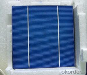
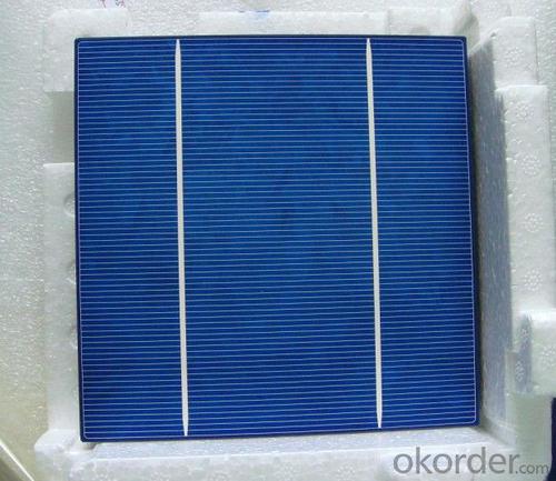


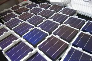
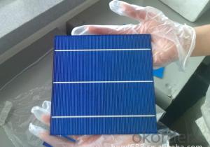
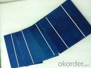
A Silicon Wafer Solar Cell - High Current 18.2% Polycrystalline Silicon Solar Cell
- Ref Price:
-

- Loading Port:
- Shanghai
- Payment Terms:
- TT OR LC
- Min Order Qty:
- 1000 pc
- Supply Capability:
- 100000 pc/month
OKorder Service Pledge
OKorder Financial Service
You Might Also Like


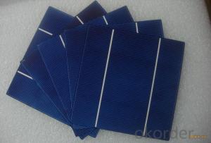
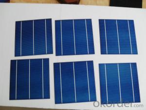
4 Bus Bars 156*156 17.6% efficiency poly solar cell
PHYSICAL CHARACTERISTICS
Dimension: 156mm x 156mm ± 0.5mm
Wafer Thickeness: 180um+20um and 200um+20um
Front(-) Four 1.2mm silver busbar
Silicon nitride blue anti-reflection coating
Back(+) aluminum back surface field
1.75mm(silver) wide segment soldering pads

Typical Electrical Characteristics
Efficiency | W(Pmpp) | V(Umpp) | A(Impp) | V(Uoc) | A(Isc) |
17.4-17.5 | 4.234 | 0.517 | 8.231 | 0.622 | 8.759 |
17.5-17.6 | 4.259 | 0.519 | 8.243 | 0.623 | 8.769 |
17.7-17.8 | 4.283 | 0.521 | 8.256 | 0.625 | 8.779 |
17.8-17.9 | 4.307 | 0.523 | 8.268 | 0.626 | 8.788 |
17.9-18.0 | 4.332 | 0.525 | 8.281 | 0.627 | 8.798 |
18.0-18.1 | 4.380 | 0.529 | 8.306 | 0.629 | 8.808 |
18.1-18.2 | 4.405 | 0.531 | 8.318 | 0.632 | 8.818 |
18.2-18.3 | 4.429 | 0.533 | 8.331 | 0.633 | 8.837 |
18.3-18.4 | 4.453 | 0.535 | 8.344 | 0.634 | 8.847 |
18.4-18.5 | 4.478 | 0.537 | 8.356 | 0.636 | 8.856 |
18.5-18.6 | 4.502 | 0.539 | 8.369 | 0.637 | 8.866 |
Efficiency | W(Pmpp) | V(Umpp) | A(Impp) | V(Uoc) | A(Isc) |
20.90-21.00 | 5.06 | 0.557 | 9.007 | 0.653 | 9.688 |
20.80-20.90 | 5.04 | 0.556 | 9.062 | 0.652 | 9.683 |
20.70-20.80 | 5.02 | 0.554 | 9.055 | 0.651 | 9.684 |
20.60-20.70 | 4.99 | 0.552 | 9.033 | 0.651 | 9.672 |
20.50-20.60 | 4.97 | 0.550 | 9.002 | 0.650 | 9.673 |
20.40-20.50 | 4.94 | 0.548 | 9.012 | 0.649 | 9.674 |
20.30-20.40 | 4.92 | 0.546 | 9.009 | 0.649 | 9.655 |
20.20-20.30 | 4.89 | 0.543 | 9.012 | 0.648 | 9.634 |
20.10-20.20 | 4.87 | 0.541 | 8.998 | 0.648 | 9.617 |
20.00-20.10 | 4.85 | 0.540 | 8.977 | 0.647 | 9.600 |
*Data under standard testing conditional (STC):1,000w/m2,AM1.5, 25°C , Pmax:Positive power tolerance.
3 Bus Bars 156*156 17.4% efficiency poly solar cell
Dimension: 156 mm x 156 mm ± 0.5 mm
Wafer Thickeness: 156 mm x 156 mm ± 0.5 mm

Typical Electrical Characteristics:
| Efficiency code | 1660 | 1680 | 1700 | 1720 | 1740 | 1760 | 1780 | 1800 | 1820 | 1840 | 1860 |
| Efficiency (%) | 16.6 | 16.8 | 17.0 | 17.2 | 17.4 | 17.6 | 17.8 | 18.0 | 18.2 | 18.4 | 18.6 |
| Pmax (W) | 4.04 | 4.09 | 4.14 | 4.19 | 4.23 | 4.28 | 4.33 | 4.38 | 4.43 | 4.48 | 4.53 |
| Voc (V) | 0.612 | 0.615 | 0.618 | 0.621 | 0.624 | 0.627 | 0.629 | 0.63 | 0.633 | 0.635 | 0.637 |
| Isc (A) | 8.42 | 8.46 | 8.51 | 8.56 | 8.61 | 8.65 | 8.69 | 8.73 | 8.77 | 8.81 | 8.84 |
| Imp (A) | 7.91 | 7.99 | 8.08 | 8.16 | 8.22 | 8.27 | 8.33 | 8.38 | 8.43 | 8.48 | 8.53 |
* Testing conditions: 1000 W/m2, AM 1.5, 25 °C, Tolerance: Efficiency ± 0.2% abs., Pmpp ±1.5% rel.
* Imin : at 0.5 V
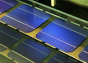
Production:

Package:

FAQ:
1. Q: Do you have your own factory?
A: Yes, we have. Our factory located in Jiangsu
2. Q: How can I visit your factory?
A: Before you visit,please contact us.We will show you the route or arrange a car to pick you up.
3. Q: Do you provide free sample?
A: Commenly we provide paid sample.
4. Q: Could you print our company LOGO on the nameplate and package?
A: Yes, we accept it.And need an Authorization Letter from you.
5. Q: Do you accept custom design on size?
A: Yes, if the size is reasonable.
6. Q: How can I be your agent in my country?
A: Please leave feedback. It's better for us to talk about details by email.
7. Q: Do you have solar project engineer who can guide me to install system?
A: Yes, we have a professional engineer team. They can teach you how to install a solar system.
- Q: What are the advantages of using silicon for solar wafers?
- There are several advantages of using silicon for solar wafers. Firstly, silicon is abundantly available and is one of the most common elements on Earth, making it cost-effective. Secondly, silicon has excellent electrical properties, such as its ability to convert sunlight into electricity efficiently. Additionally, silicon is highly stable and durable, ensuring a longer lifespan for solar panels. Lastly, silicon can be easily processed and fabricated into wafers, making it a versatile material for solar cell production.
- Q: How are defects in solar silicon wafers detected and minimized?
- Defects in solar silicon wafers are primarily detected and minimized through rigorous quality control processes. Optical inspection techniques such as visual inspections, infrared imaging, and photoluminescence imaging are commonly used to identify defects such as cracks, impurities, and dislocations in the wafers. Additionally, advanced testing methods like electron microscopy, X-ray diffraction, and spectroscopy are employed to further analyze and characterize the defects. To minimize defects, manufacturers adopt strict production protocols, including purification of the silicon feedstock, controlling the manufacturing environment, and implementing advanced manufacturing techniques like zone melting and Czochralski growth. These measures ensure the production of high-quality silicon wafers with minimal defects, leading to enhanced efficiency and reliability in solar cells.
- Q: Can solar silicon wafers be used in other applications besides solar energy?
- Yes, solar silicon wafers can be used in other applications besides solar energy. They can be utilized in electronic devices such as semiconductors, integrated circuits, and sensors. Additionally, they can be used in the production of photovoltaic cells for various electronic devices, including calculators and watches.
- Q: Seeking for the video: manual insert silicon wafer single crystal insert method
- To solve the finger print is very simple, as long as the requirements of employees can not in the whole process of operation of the silicon bare hand contact can be, no debris is not possible, but to see the machine or man-made debris or before the procedure is cracked as, if it is man-made debris, to do a a standard specification, as long as the control that would reduce the rate of fragmentation. Or artificial debris to staff assessment, but also meet the results. I used to track debris for a long time, when all of the pieces are controlled by the descendants of the debris is very low. The main road is the most hidden crack. If the semi automatic equipment under normal circumstances will not produce debris, such as automatic equipment, such as degumming equipment will produce debris, mainly the spray pressure is too large, but the pressure is also very little fragmentation of the right. I think the main thing is to see if you have asked the staff how to do it, followed by the implementation of your employees are required. You can look at these lines on the line!
- Q: Can solar silicon wafers be used in solar-powered military applications?
- Yes, solar silicon wafers can be used in solar-powered military applications. They are commonly used in various military systems, including remote surveillance equipment, communication devices, and portable power solutions for soldiers in the field. Solar-powered military applications benefit from the reliability, durability, and energy efficiency of solar silicon wafers, making them a viable option for sustainable power generation in military operations.
- Q: What is the production capacity of solar silicon wafers worldwide?
- As of 2021, the global production capacity of solar silicon wafers is estimated to be around 200 gigawatts (GW) per year.
- Q: How are solar silicon wafers packaged for transportation and installation?
- Solar silicon wafers are typically packaged for transportation and installation in protective materials such as foam or plastic trays. These trays are designed to hold multiple wafers securely and prevent damage during transit. Additionally, the wafers are often further protected by placing them in cardboard boxes or crates, which provide additional stability and safeguard against any potential impact during transportation.
- Q: Are there any limitations to the size of solar silicon wafers?
- Yes, there are limitations to the size of solar silicon wafers. Currently, the most common size for solar silicon wafers is around 156 mm x 156 mm or 6 inches x 6 inches. This size is widely used in the solar industry due to various factors such as manufacturing capabilities, handling, and compatibility with existing solar cell production equipment. However, larger wafer sizes, such as 166 mm x 166 mm or even larger, are being developed and implemented to increase solar panel efficiency and reduce manufacturing costs. Nonetheless, there are practical limitations to the size of solar silicon wafers, including the challenges related to handling larger sizes, potential increase in material waste, and compatibility with existing solar panel designs and installations.
- Q: How is a conversion efficiency measured in a solar silicon wafer?
- A conversion efficiency in a solar silicon wafer is typically measured by comparing the amount of sunlight energy that is converted into usable electricity by the solar cell, divided by the total amount of sunlight energy that falls on the solar cell. This ratio is expressed as a percentage and provides a measure of how effectively the solar cell converts sunlight into electricity.
- Q: Can solar silicon wafers be used in all types of solar panels?
- Yes, solar silicon wafers can be used in all types of solar panels. Silicon is the most commonly used material for solar panels, and it can be processed into wafers and used in various types of solar panel technologies such as monocrystalline, polycrystalline, and thin-film.
Send your message to us
A Silicon Wafer Solar Cell - High Current 18.2% Polycrystalline Silicon Solar Cell
- Ref Price:
-
- Loading Port:
- Shanghai
- Payment Terms:
- TT OR LC
- Min Order Qty:
- 1000 pc
- Supply Capability:
- 100000 pc/month
OKorder Service Pledge
OKorder Financial Service
Similar products


Hot products


Hot Searches
Related keywords

