


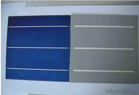

6 inch Multi Solar Silicon Wafer -- 156 x 156 mm by Solar Silicon Wafer Manufacturers
- Ref Price:
-

- Loading Port:
- China main port
- Payment Terms:
- TT OR LC
- Min Order Qty:
- 100 watt
- Supply Capability:
- 10000 watt/month
OKorder Service Pledge
OKorder Financial Service
You Might Also Like


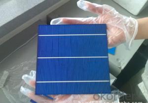
6 Inch Multi Solar Cell -- 156 x 156 mm
FEATURES
`Long Service Life
`High Efficiency Solar Cells
`Special Aluminum Frame Design
`High Transmission, Low Iron Tempered Glass
`Advanced Cell Encapsulation
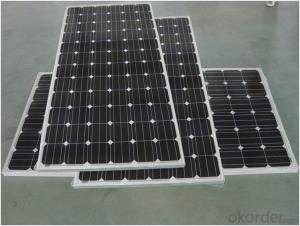
Solar Module Specifications
Mono 80W—100W
Module | Type (36 Series) | |||||
Encapsulation | Glass/EVA/Cells/EVA/TPT | |||||
Parameters | SNM-M80(36) | SNM-M85(36) | SNM-M90(36) | SNM-M95(36) | SNM-M100(36) | |
Max power | Pm(W) | 80W | 85W | 90W | 95W | 100W |
Tolerance | +/-3% | |||||
Open circuit voltage | Voc(V) | 21.2 | 21.8 | 21.8 | 22.3 | 22.6 |
Short circuit current | Isc(A) | 4.84 | 5.00 | 5.30 | 5.44 | 5.68 |
Max. power voltage | Vmp(V) | 17.5 | 18.0 | 18.0 | 18.5 | 18.5 |
Max. power current | Imp(A) | 4.57 | 4.72 | 5.00 | 5.14 | 5.40 |
Dimensions | (L*W*H) | 1200x540x35mm | ||||
Net Weight | (kg) | 9 | ||||
Max. system voltage | (V) | 1000VDC | ||||
Operate Temp. Scope | -40/+85'C | |||||
Resistance | 227g steel ball fall down from 1m height and 120m/s wind | |||||
Warranty | Pm is no less 90% in 10 years and no less 80% in 25 years | |||||
STC | (Standard Test Condition: 1000W/m2, AM1.5, and 25'C) | |||||
Picture show


- Q: What is the role of solar silicon wafers in reducing carbon emissions?
- Solar silicon wafers play a crucial role in reducing carbon emissions by serving as the foundation for solar photovoltaic (PV) cells. These wafers are made from purified silicon, which enables the conversion of sunlight into electricity. By harnessing solar energy, PV cells generate clean and renewable electricity without emitting greenhouse gases or other harmful pollutants. Consequently, widespread adoption of solar silicon wafers and PV cells in solar panels helps to offset the use of fossil fuels for electricity generation, thereby reducing carbon emissions and mitigating climate change.
- Q: How do solar silicon wafers perform in sandy environments?
- Solar silicon wafers perform well in sandy environments due to their durable construction and protective coatings. They are designed to withstand harsh conditions, including exposure to sand and dust particles. However, regular cleaning and maintenance are essential to ensure optimal performance and prevent any potential efficiency loss caused by the accumulation of sand on the surface of the panels.
- Q: Are solar silicon wafers affected by chemical exposure?
- Yes, solar silicon wafers can be affected by chemical exposure. Chemicals, such as certain acids or solvents, can corrode or etch the surface of the wafers, leading to reduced efficiency or even failure of the solar cells. It is important to handle and store solar silicon wafers properly to avoid chemical damage.
- Q: How are solar silicon wafers coated to prevent reflection losses?
- Solar silicon wafers are coated with an anti-reflective (AR) coating to minimize reflection losses. This coating is typically a thin film of materials such as silicon nitride or titanium dioxide, which have a low refractive index. The AR coating helps to reduce the amount of sunlight that is reflected away from the surface of the wafer, allowing more light to be absorbed and converted into electricity.
- Q: How is a solar silicon wafer tested for quality control?
- A solar silicon wafer is tested for quality control through various processes, including visual inspection, electrical measurements, and material characterization. Visual inspection involves checking for any physical defects such as cracks, scratches, or impurities on the wafer's surface. Electrical measurements are conducted to assess the wafer's performance, including parameters like resistivity, efficiency, and output power. Material characterization techniques like spectroscopy and microscopy are used to analyze the composition, crystalline structure, and purity of the wafer. These quality control tests ensure that only wafers meeting the desired standards are used in solar cell production.
- Q: Can solar silicon wafers be used in marine or offshore applications?
- Yes, solar silicon wafers can be used in marine or offshore applications. However, special considerations need to be taken into account due to the harsh marine environment, such as protection against corrosion, water resistance, and durability against high winds and saltwater exposure.
- Q: What is the impact of impurities on the durability of solar silicon wafers?
- Impurities in solar silicon wafers can have a significant impact on their durability. These impurities can affect the structural integrity and electrical properties of the wafers, leading to reduced efficiency and shorter lifespan of the solar cells. Impurities like metal ions or oxygen can introduce defects in the crystal lattice, causing degradation and increased recombination of charge carriers. This can result in reduced power output and decreased overall performance of the solar panels. Therefore, minimizing impurities and ensuring high purity silicon is crucial for enhancing the durability and longevity of solar silicon wafers.
- Q: Are there any government regulations or standards for solar silicon wafers?
- Yes, there are government regulations and standards for solar silicon wafers. These regulations and standards are put in place by various governmental bodies to ensure the quality, efficiency, and safety of solar silicon wafers used in the production of solar panels. These regulations may include specifications on the purity, dimensions, chemical composition, and electrical properties of silicon wafers. Compliance with these regulations and standards is necessary for manufacturers to maintain industry standards and meet the requirements for government incentives or certifications.
- Q: What are the main factors that affect the lifespan of a solar silicon wafer?
- The main factors that affect the lifespan of a solar silicon wafer include the quality of the silicon material used, the manufacturing process, exposure to external factors such as temperature and humidity, and the level of stress the wafer is subjected to during operation. Additionally, proper handling, installation, and maintenance practices also play a significant role in determining the lifespan of a solar silicon wafer.
- Q: How do solar silicon wafers perform in high-pollution environments?
- Solar silicon wafers generally perform well in high-pollution environments. While pollution can potentially reduce the efficiency of solar panels over time by decreasing the amount of sunlight reaching the cells, manufacturers have taken measures to mitigate this impact. Anti-reflective coatings and regular cleaning can help maintain optimal performance. Additionally, advancements in technology and materials have made solar panels more resilient to pollution, enabling them to continue generating electricity effectively even in polluted areas.
Send your message to us
6 inch Multi Solar Silicon Wafer -- 156 x 156 mm by Solar Silicon Wafer Manufacturers
- Ref Price:
-
- Loading Port:
- China main port
- Payment Terms:
- TT OR LC
- Min Order Qty:
- 100 watt
- Supply Capability:
- 10000 watt/month
OKorder Service Pledge
OKorder Financial Service
Similar products


Hot products


Hot Searches
Related keywords

