


Solar Grade Silicon Wafer - High Quality A Grade Polycrystalline 5V 17.4% Solar Cell
- Ref Price:
-

- Loading Port:
- Shanghai
- Payment Terms:
- TT OR LC
- Min Order Qty:
- 1000 pc
- Supply Capability:
- 100000 pc/month
OKorder Service Pledge
OKorder Financial Service
You Might Also Like


Specifications
hot sale solar cell
1.16.8%~18.25% high efficiency
2.100% checked quality
3.ISO9001/ISO14001/TUV/CE/UL
4.stable performance
We can offer you the best quality products and services, don't miss !
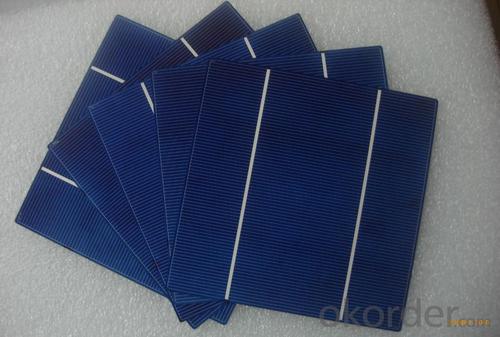
POLY6'(156*156)
Polycrystalline Silicon Solar cell
Physical Characteristics
Dimension: 156mm×156mm±0.5mm
Diagonal: 220mm±0.5mm
Thickness(Si): 200±20 μm
Front(-) Back(+)
Blue anti-reflecting coating (silicon nitride); Aluminum back surface field;
1.5mm wide bus bars; 2.0mm wide soldering pads;
Distance between bus bars: 51mm . Distance between bus bars :51mm .
Electrical Characteristics
Efficiency(%) | 18.00 | 17.80 | 17.60 | 17.40 | 17.20 | 16.80 | 16.60 | 16.40 | 16.20 | 16.00 | 15.80 | 15.60 |
Pmpp(W) | 4.33 | 4.29 | 4.24 | 4.19 | 4.14 | 4.09 | 4.04 | 3.99 | 3.94 | 3.90 | 3.86 | 3.82 |
Umpp(V) | 0.530 | 0.527 | 0.524 | 0.521 | 0.518 | 0.516 | 0.514 | 0.511 | 0.509 | 0.506 | 0.503 | 0.501 |
Impp(A) | 8.159 | 8.126 | 8.081 | 8.035 | 7.990 | 7.938 | 7.876 | 7.813 | 7.754 | 7.698 | 7.642 | 7.586 |
Uoc(V) | 0.633 | 0.631 | 0.628 | 0.625 | 0.623 | 0.620 | 0.618 | 0.617 | 0.615 | 0.613 | 0.611 | 0.609 |
Isc(A) | 8.709 | 8.677 | 8.629 | 8.578 | 8.531 | 8.478 | 8.419 | 8.356 | 8.289 | 8.220 | 8.151 | 8.083 |

MONO5'(125*125mm)165
Monocrystalline silicon solar cell
Physical Characteristics
Dimension: 125mm×125mm±0.5mm
Diagonal: 165mm±0.5mm
Thickness(Si): 200±20 μm
Front(-) Back(+)
Blue anti-reflecting coating(silicon nitride); Aluminum back surface field;
1.6mmwide bus bars; 2.5mm wide soldering pads;
Distance between bus bars: 61mm . Distance between bus bars :61mm .
Electrical Characteristics
Efficiency(%) | 19.40 | 19.20 | 19.00 | 18.80 | 18.60 | 18.40 | 18.20 | 18.00 | 17.80 | 17.60 | 17.40 | 17.20 |
Pmpp(W) | 2.97 | 2.94 | 2.91 | 2.88 | 2.85 | 2.82 | 2.79 | 2.76 | 2.73 | 2.70 | 2.67 | 2.62 |
Umpp(V) | 0.537 | 0.535 | 0.533 | 0.531 | 0.527 | 0.524 | 0.521 | 0.518 | 0.516 | 0.515 | 0.513 | 0.509 |
Impp(A) | 5.531 | 5.495 | 5.460 | 5.424 | 5.408 | 5.382 | 5.355 | 5.328 | 5.291 | 5.243 | 5.195 | 4.147 |
Uoc(V) | 0.637 | 0.637 | 0.636 | 0.635 | 0.633 | 0.630 | 0.629 | 0.629 | 0.628 | 0.626 | 0.626 | 0.625 |
Isc(A) | 5.888 | 5.876 | 5.862 | 5.848 | 5.839 | 5.826 | 5.809 | 5.791 | 5.779 | 5.756 | 5.293 | 5.144 |

FAQ:
Q:How can i get some sample?
A:Yes , if you want order ,sample is not a problem.
Q:How about your solar panel efficency?
A: Our product efficency around 17.25%~18.25%.
Q:What’s the certificate you have got?
A: we have overall product certificate of ISO9001/ISO14001/CE/TUV/UL
- Q: What is the role of a junction box connector in a solar silicon wafer?
- A junction box connector in a solar silicon wafer serves the important role of providing a connection point for the electrical wires that transmit the generated solar energy. It ensures a secure and reliable electrical connection between the solar cells and the external electrical system, such as inverters or batteries. Additionally, the junction box connector may incorporate diodes or other protective devices to prevent reverse current flow and protect the solar panel from potential damage.
- Q: How are solar silicon wafers protected from degradation over time?
- Solar silicon wafers are protected from degradation over time through the use of various protective coatings and encapsulation techniques. One common method is the application of anti-reflective coatings that not only enhance the efficiency of the solar cells but also act as a barrier against environmental factors such as moisture, dust, and ultraviolet (UV) radiation. Additionally, the wafers are often encapsulated within a durable and weather-resistant material, such as tempered glass or polymer, which shields them from physical damage and prolongs their lifespan. These measures ensure that solar silicon wafers remain robust and perform optimally even after prolonged exposure to harsh weather conditions and other potential degrading factors.
- Q: Can solar silicon wafers be used in disaster response vehicles?
- Yes, solar silicon wafers can be used in disaster response vehicles. They can be used to harness solar energy and power various systems and equipment in these vehicles, providing a sustainable and reliable source of power during emergency situations.
- Q: Are there any advancements in solar silicon wafer recycling technologies?
- Yes, there have been significant advancements in solar silicon wafer recycling technologies. With the increasing demand for renewable energy, researchers and companies have been working on developing more efficient and cost-effective methods to recycle silicon wafers used in solar panels. These advancements include improved separation and purification techniques, innovative recycling processes, and the development of new technologies to extract valuable materials from used solar panels. These advancements not only help reduce the environmental impact of solar panel production but also contribute to the circular economy by recovering valuable resources for reuse.
- Q: Solar silicon wafer cutting fluid content is polyethylene glycol, flash point 182-278 DEG C, saturated vapor pressure of 6.21KPa/20 C / C in storage in the barrel, after exposure, its volatile gas is harmful?
- Combustible gas is hydrogen is not polyethylene glycol, but no matter because of ventilation, ventilation, to avoid the closed environment in the case of an open flame on the line
- Q: Process flow of wafer wafer ultrasonic cleaning machine?
- Plasma cleaning method, which is characterized in that the process parameters of gas flushing process is: the chamber pressure of 15 mTorr, process gas flow 300sccm, time 3S; process parameters of starting process is: the chamber pressure of 15 mTorr, process gas flow on the electrode 300sccm, power 300W, time Ss
- Q: Are solar silicon wafers affected by voltage fluctuations?
- Yes, solar silicon wafers can be affected by voltage fluctuations. Fluctuations in voltage can impact the performance and efficiency of solar panels, as they rely on a stable and consistent voltage to generate electricity. Variations in voltage can cause fluctuations in current, which can lead to reduced power output or even damage to the solar cells. Therefore, it is important to ensure a stable and well-regulated voltage supply for optimal performance of solar silicon wafers.
- Q: From raw materials to finished products processing and production of the main links? Construction technology? Key issues of safety in production? What security measures are generally taken?
- Another reason is that CZ is easier to produce large size single crystal silicon rods than FZ method. At present, using the method of CZ CZ main equipment: CZ growth furnace growth furnace by CZ components can be divided into four parts: (1) the furnace body comprises a quartz crucible, graphite crucible, heating and insulating element in the furnace wall (2) crystal and crucible for rotary mechanism: including seed chuck, hanging and pulled the rotating element (3) atmosphere pressure control: including gas flow control, vacuum system and pressure control valve (4) control system: including the detection sensor and computer control system processing: charging, melting, necking, shoulder growth, growth, growth and diameter growth of the tail (1) charging: the polysilicon raw materials and impurities in the quartz crucible, the type of impurity depends on the N or P type resistance. Boron, phosphorus, antimony, arsenic. (2): after the melting quartz crucible for polysilicon feedstock after long crystal furnace must be closed and vacuum filling in high purity argon to maintain a certain pressure range, and then open the graphite heater power supply, heating to the melting temperature (1420 DEG C) above, the polysilicon raw material melting. (3) necking growth: when the temperature of the silicon melt is stable, the seed is slowly immersed in the silicon melt. Because of the thermal stress in the contact between the seed and the silicon melt, the seeds will be dislocation, which must be used to reduce the growth of the crystal. Necking is the seed growth will rapidly upward, the seed crystal grows to a certain size of the reduced diameter (4-6mm) due to the dislocation line and growth axis into a corner, as long as the neck is long enough, the dislocation can grow the crystal surface, zero crystal dislocation.
- Q: How do solar silicon wafers perform in desert environments?
- Solar silicon wafers perform well in desert environments due to the high levels of sunlight and low humidity. The dry and hot conditions in deserts allow for efficient solar energy generation, as there are fewer obstructions such as clouds or pollution. However, it is important to ensure proper maintenance and cleaning of the wafers to prevent the accumulation of dust or sand particles, which can hinder their performance.
- Q: Can solar silicon wafers be used in solar-powered security systems?
- Yes, solar silicon wafers can be used in solar-powered security systems. These wafers are commonly used in the production of solar cells, which convert sunlight into electricity. By harnessing solar energy, security systems can operate independently, without relying on grid power or batteries. Solar silicon wafers provide a reliable and sustainable solution for powering security systems, ensuring continuous surveillance even in remote or off-grid locations.
Send your message to us
Solar Grade Silicon Wafer - High Quality A Grade Polycrystalline 5V 17.4% Solar Cell
- Ref Price:
-
- Loading Port:
- Shanghai
- Payment Terms:
- TT OR LC
- Min Order Qty:
- 1000 pc
- Supply Capability:
- 100000 pc/month
OKorder Service Pledge
OKorder Financial Service
Similar products


Hot products


Hot Searches
Related keywords

