


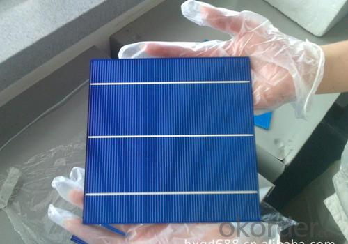

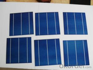
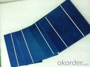
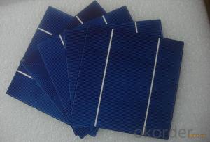
Silicon Wafer Based High Current 17.4% Polycrystalline Silicon Solar Cells
- Ref Price:
-

- Loading Port:
- Shanghai
- Payment Terms:
- TT OR LC
- Min Order Qty:
- 1000 pc
- Supply Capability:
- 100000 pc/month
OKorder Service Pledge
OKorder Financial Service
You Might Also Like


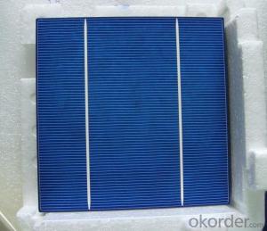
4 Bus Bars 156*156 17.6% efficiency poly solar cell
PHYSICAL CHARACTERISTICS
Dimension: 156mm x 156mm ± 0.5mm
Wafer Thickeness: 180um+20um and 200um+20um
Front(-) Four 1.2mm silver busbar
Silicon nitride blue anti-reflection coating
Back(+) aluminum back surface field
1.75mm(silver) wide segment soldering pads

Typical Electrical Characteristics
Efficiency | W(Pmpp) | V(Umpp) | A(Impp) | V(Uoc) | A(Isc) |
17.4-17.5 | 4.234 | 0.517 | 8.231 | 0.622 | 8.759 |
17.5-17.6 | 4.259 | 0.519 | 8.243 | 0.623 | 8.769 |
17.7-17.8 | 4.283 | 0.521 | 8.256 | 0.625 | 8.779 |
17.8-17.9 | 4.307 | 0.523 | 8.268 | 0.626 | 8.788 |
17.9-18.0 | 4.332 | 0.525 | 8.281 | 0.627 | 8.798 |
18.0-18.1 | 4.380 | 0.529 | 8.306 | 0.629 | 8.808 |
18.1-18.2 | 4.405 | 0.531 | 8.318 | 0.632 | 8.818 |
18.2-18.3 | 4.429 | 0.533 | 8.331 | 0.633 | 8.837 |
18.3-18.4 | 4.453 | 0.535 | 8.344 | 0.634 | 8.847 |
18.4-18.5 | 4.478 | 0.537 | 8.356 | 0.636 | 8.856 |
18.5-18.6 | 4.502 | 0.539 | 8.369 | 0.637 | 8.866 |
Efficiency | W(Pmpp) | V(Umpp) | A(Impp) | V(Uoc) | A(Isc) |
20.90-21.00 | 5.06 | 0.557 | 9.007 | 0.653 | 9.688 |
20.80-20.90 | 5.04 | 0.556 | 9.062 | 0.652 | 9.683 |
20.70-20.80 | 5.02 | 0.554 | 9.055 | 0.651 | 9.684 |
20.60-20.70 | 4.99 | 0.552 | 9.033 | 0.651 | 9.672 |
20.50-20.60 | 4.97 | 0.550 | 9.002 | 0.650 | 9.673 |
20.40-20.50 | 4.94 | 0.548 | 9.012 | 0.649 | 9.674 |
20.30-20.40 | 4.92 | 0.546 | 9.009 | 0.649 | 9.655 |
20.20-20.30 | 4.89 | 0.543 | 9.012 | 0.648 | 9.634 |
20.10-20.20 | 4.87 | 0.541 | 8.998 | 0.648 | 9.617 |
20.00-20.10 | 4.85 | 0.540 | 8.977 | 0.647 | 9.600 |
*Data under standard testing conditional (STC):1,000w/m2,AM1.5, 25°C , Pmax:Positive power tolerance.
3 Bus Bars 156*156 17.4% efficiency poly solar cell
Dimension: 156 mm x 156 mm ± 0.5 mm
Wafer Thickeness: 156 mm x 156 mm ± 0.5 mm

Typical Electrical Characteristics:
| Efficiency code | 1660 | 1680 | 1700 | 1720 | 1740 | 1760 | 1780 | 1800 | 1820 | 1840 | 1860 |
| Efficiency (%) | 16.6 | 16.8 | 17.0 | 17.2 | 17.4 | 17.6 | 17.8 | 18.0 | 18.2 | 18.4 | 18.6 |
| Pmax (W) | 4.04 | 4.09 | 4.14 | 4.19 | 4.23 | 4.28 | 4.33 | 4.38 | 4.43 | 4.48 | 4.53 |
| Voc (V) | 0.612 | 0.615 | 0.618 | 0.621 | 0.624 | 0.627 | 0.629 | 0.63 | 0.633 | 0.635 | 0.637 |
| Isc (A) | 8.42 | 8.46 | 8.51 | 8.56 | 8.61 | 8.65 | 8.69 | 8.73 | 8.77 | 8.81 | 8.84 |
| Imp (A) | 7.91 | 7.99 | 8.08 | 8.16 | 8.22 | 8.27 | 8.33 | 8.38 | 8.43 | 8.48 | 8.53 |
* Testing conditions: 1000 W/m2, AM 1.5, 25 °C, Tolerance: Efficiency ± 0.2% abs., Pmpp ±1.5% rel.
* Imin : at 0.5 V
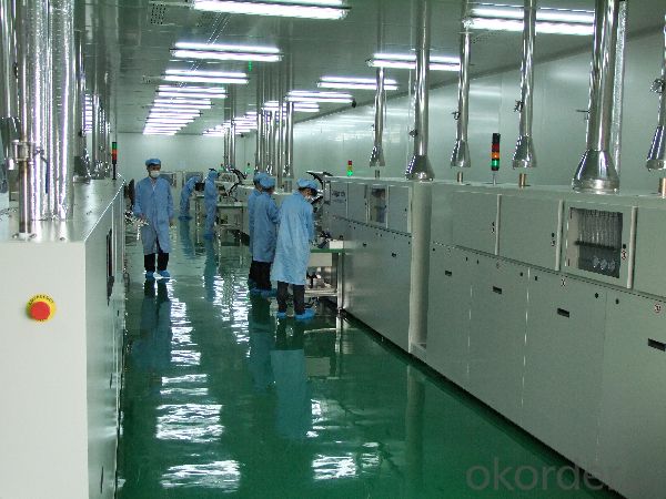
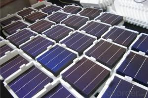
Production:

Package:

FAQ:
1. Q: Do you have your own factory?
A: Yes, we have. Our factory located in Jiangsu
2. Q: How can I visit your factory?
A: Before you visit,please contact us.We will show you the route or arrange a car to pick you up.
3. Q: Do you provide free sample?
A: Commenly we provide paid sample.
4. Q: Could you print our company LOGO on the nameplate and package?
A: Yes, we accept it.And need an Authorization Letter from you.
5. Q: Do you accept custom design on size?
A: Yes, if the size is reasonable.
6. Q: How can I be your agent in my country?
A: Please leave feedback. It's better for us to talk about details by email.
7. Q: Do you have solar project engineer who can guide me to install system?
A: Yes, we have a professional engineer team. They can teach you how to install a solar system.
- Q: What is the role of back contact in solar silicon wafers?
- The role of back contact in solar silicon wafers is to provide electrical connectivity and support for the wafer. It helps in collecting the generated electricity from the front surface of the wafer and transferring it to the external circuit. Additionally, the back contact also acts as a structural element, providing stability and rigidity to the wafer.
- Q: What is the role of surface recombination velocity on solar silicon wafers?
- The surface recombination velocity on solar silicon wafers plays a crucial role in determining the efficiency of solar cells. It refers to the rate at which charge carriers (electrons and holes) recombine at the surface of the wafer. A high surface recombination velocity leads to increased recombination, resulting in a loss of generated carriers and reduced cell efficiency. Therefore, minimizing the surface recombination velocity is essential to enhance the performance of solar cells by maximizing carrier collection and reducing energy losses.
- Q: How do solar silicon wafers perform in sandy environments?
- Solar silicon wafers perform well in sandy environments as they are designed to be highly durable and resistant to various environmental conditions. The solid construction and protective coatings of the wafers help minimize the negative effects of sand particles, such as scratching or obstructing the surface. However, it is still important to regularly clean the panels to maintain optimal performance and ensure that sand accumulation does not significantly reduce their efficiency.
- Q: What is the typical reflectivity of a solar silicon wafer?
- The typical reflectivity of a solar silicon wafer is around 30% to 40%.
- Q: Are there any initiatives to reduce the cost of solar silicon wafers?
- Yes, there are several initiatives underway to reduce the cost of solar silicon wafers. These initiatives include advancements in manufacturing processes, research and development of new materials, and improvements in production efficiency. Additionally, governments and organizations are providing financial support and incentives to promote the adoption of solar energy, which indirectly helps in reducing the cost of solar silicon wafers.
- Q: Why do monocrystalline silicon chamfer? Polysilicon film?
- There are many single crystal chamfer.Single crystals are generally large chamfer, there is a single crystal process decision. There is a single crystal silicon rod is cut out, in order to make full use of the silicon rod, appear large chamfer; and polycrystalline is generally small chamfer, is to reduce the crack edge of the silicon wafer, the external stress of the silicon wafer or cell rupture. Polycrystalline battery will also appear large chamfer, those are generally small chamfer of the battery, found that there is a problem after the cut into large chamfer.
- Q: How do solar silicon wafers perform in high-wind conditions?
- Solar silicon wafers are generally designed to withstand high-wind conditions without significant damage. However, it is important to note that excessive wind speeds can potentially cause some stress or flexing on solar panels, including the silicon wafers. To ensure their performance and durability, solar panels are typically engineered with robust frames and mounting systems that can withstand strong winds. Additionally, regular maintenance and inspections are recommended to identify any potential issues and ensure the panels are properly secured.
- Q: What is the impact of microcracks in solar silicon wafers on performance?
- Microcracks in solar silicon wafers can have a significant impact on the performance of solar cells. These cracks can weaken the structural integrity of the wafer, leading to potential breakage or delamination. Moreover, microcracks can increase the chances of moisture ingress, causing corrosion and degradation of the solar cell. Additionally, these cracks can impede the flow of electrons, reducing the efficiency of the solar panel and overall power output. Therefore, it is crucial to minimize or eliminate microcracks to ensure optimal performance and longevity of solar silicon wafers.
- Q: What is the purpose of a temperature coefficient in a solar silicon wafer?
- The purpose of a temperature coefficient in a solar silicon wafer is to measure the change in electrical performance of the wafer with respect to temperature. It helps in understanding how the efficiency of the solar cell is affected by temperature variations. By knowing the temperature coefficient, manufacturers and users can determine the optimal operating conditions for the solar cell and make necessary adjustments to maximize its output and lifespan.
- Q: One hundred watts of solar panels to how many pieces of silicon wafers, 156 of single crystals and polycrystalline
- As for the power, according to the W=UI formula can be obtained, since a single voltage is fixed, the resulting current size determines the power of a battery, the current per tablet produced is not fixed, with the conversion rate of the conversion rate, high current is large, the reverse is small; the same the power conversion rate is high, the area is small
Send your message to us
Silicon Wafer Based High Current 17.4% Polycrystalline Silicon Solar Cells
- Ref Price:
-
- Loading Port:
- Shanghai
- Payment Terms:
- TT OR LC
- Min Order Qty:
- 1000 pc
- Supply Capability:
- 100000 pc/month
OKorder Service Pledge
OKorder Financial Service
Similar products

Hot products


Hot Searches
Related keywords

