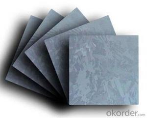
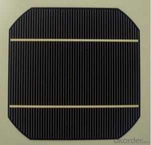
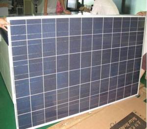
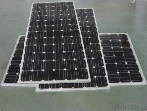
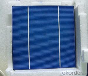
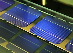
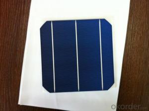
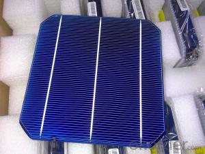
Silicon Solar Wafer - Mono Solar Cells 156mm*156mm in Bulk Quantity Low Price Stock 19.0
- Loading Port:
- Shanghai
- Payment Terms:
- TT OR LC
- Min Order Qty:
- 1000 pc
- Supply Capability:
- 100000 pc/month
OKorder Service Pledge
OKorder Financial Service
You Might Also Like
Brief Introduction
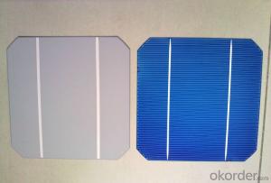
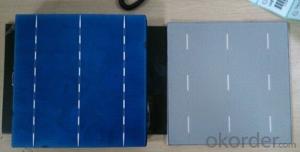
- Up to 20.0% efficiency, one of the highest performing mono crystalline cells on the market
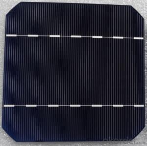
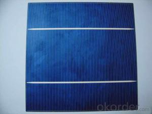
- Three bus bars boosts current collection over the entire cell area, leading to higher fill factors
- Blue anti-reflecting coating allows more sunlight be captured and converted to electricity
- Finer, closer fingers improves charge collections for improved energy yield
- Lower light-induced degradation leads to greater power output over the entire module lifetime
- All solar cells are tightly classified to optimize output of module
- Maximum yield and longevity due to hotspot prevention
- Premium appearance results in a highly uniform and aesthetically appealing module
Specification
- Product Mono-crystalline silicon solar cell
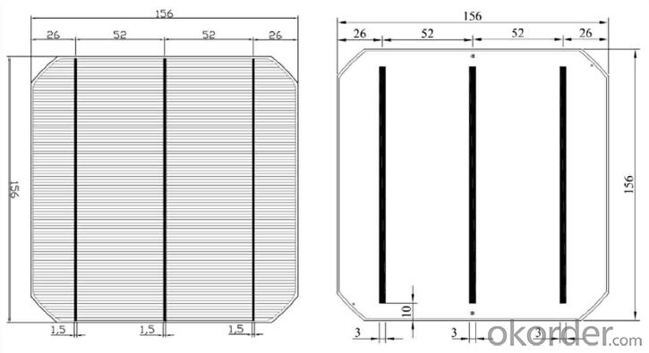
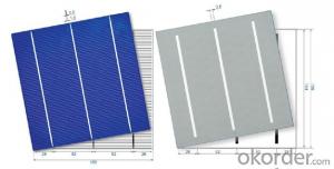
- Dimension 156 mm x 156 mm ± 0.5 mm
- Thickness 200 μm ± 30 μm
- Front 1.5 ± 0.1 mm busbar (silver)
- Silicon nitride antireflection coating
- Back 3.0 mm continuous soldering pads (silver)
- Back surface field (aluminum)
Electric performance parameters

- Testing conditions: 1000 W/m2, AM 1.5, 25 °C, Tolerance: Efficiency ± 0.2% abs., Pmpp ±1.5% rel.
- Imin : at 0.5 V
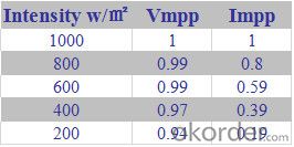
Light Intensity Dependence
Soldering Ability
- Peel Strength: > 1.0 N/mm (Pull soldered ribbon from busbar in 5 mm/s of 180°)
Dimension Figure

Quick Response
- Any time and anywhere, reply clients' email and solve all problems happen in the work at the first time.
- Remove clients doubts and offer the best solution at the first time.
- Give our clients the lastest news of the photovoltaic, update the newest stock informtion.
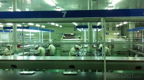
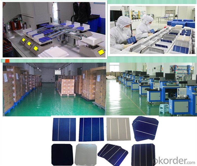
Production and Quality Control
- Precision cell efficiency sorting procedures
- Stringent criteria for color uniformity and appearance
- Reverse current and shunt resistance screening
- ISO9001,ISO14001 and OHSAS 18001,TUV Certificated

FAQ:
1. Q: Do you have your own factory?
A: Yes, we have. Our factory located in Jiangsu
2. Q: How can I visit your factory?
A: Before you visit,please contact us.We will show you the route or arrange a car to pick you up.
3. Q: Do you provide free sample?
A: Commenly we provide paid sample.
4. Q: Could you print our company LOGO on the nameplate and package?
A: Yes, we accept it.And need an Authorization Letter from you.
5. Q: Do you accept custom design on size?
A: Yes, if the size is reasonable.
6. Q: How can I be your agent in my country?
A: Please leave feedback. It's better for us to talk about details by email.
7. Q: Do you have solar project engineer who can guide me to install system?
A: Yes, we have a professional engineer team. They can teach you how to install a solar system.
- Q: What is the role of antireflection coatings on solar silicon wafers?
- The role of antireflection coatings on solar silicon wafers is to minimize the reflection of sunlight and increase the absorption of light by the silicon material. This improves the overall efficiency of the solar cell by allowing more light to be converted into electricity.
- Q: Can solar silicon wafers be used in solar water heating systems?
- Yes, solar silicon wafers can be used in solar water heating systems. These wafers are typically used in the production of photovoltaic (PV) solar panels, which convert sunlight into electricity. However, in solar water heating systems, the solar silicon wafers are used to capture the sun's heat to directly heat water.
- Q: How to make monocrystalline silicon solar panels? Begged: specific steps
- Phosphate glassThe process is used for solar cell production in the manufacturing process, through chemical etching silicon that is immersed in hydrofluoric acid solution, complexes six fluorosilicic acid to produce chemical reaction to produce soluble phosphorus silicon glass layer, a diffusion system to remove the node after the formation of the surface of the silicon wafer. In the diffusion process, POCL3 reacts with O2 to form P2O5 on the surface of silicon wafer. P2O5 reacted with Si to produce SiO2 and phosphorus atoms, which form a layer of phosphorus containing SiO2 on the surface of the silicon wafer. Removing phosphorosilicate glass equipment is generally composed of a main body, a cleaning tank, manipulator, servo drive system, electric control system and the automatic mixing acid system components, the main power source of hydrofluoric acid, nitrogen, compressed air, water, wastewater and exhaust heat. Hydrofluoric acid is capable of dissolving silicon dioxide because of the reaction of hydrofluoric acid and silica to produce volatile four fluorinated silicon gas. If the hydrofluoric acid is too heavy, the reaction of four fluorinated silicon will further react with hydrofluoric acid to produce soluble complex and the material of the six fluorine acid.
- Q: What are the main differences between monocrystalline and polycrystalline solar silicon wafers?
- The main differences between monocrystalline and polycrystalline solar silicon wafers are in their crystal structure and efficiency. Monocrystalline wafers are made from a single crystal structure, resulting in a uniform and high-purity material. This allows them to have higher efficiency and power output. On the other hand, polycrystalline wafers are made from multiple crystal structures, resulting in a less uniform material with lower efficiency. However, polycrystalline wafers are generally less expensive to produce.
- Q: How are solar silicon wafers protected from handling-induced microcracks?
- Solar silicon wafers are protected from handling-induced microcracks through several measures. Firstly, they are usually coated with a thin layer of protective material, such as a polymer film or glass, which serves as a physical barrier against potential damage during handling. Additionally, manufacturers employ advanced manufacturing techniques to strengthen the wafer's structure, making it more resistant to microcracks. These techniques may include doping the silicon with specific impurities or applying stress-reducing treatments. Finally, strict handling protocols are implemented, ensuring that the wafers are carefully transported and manipulated to minimize the risk of microcracks.
- Q: How do solar silicon wafers affect the overall flexibility of a solar panel?
- Solar silicon wafers do not directly affect the overall flexibility of a solar panel. The flexibility of a solar panel depends on the material and design of the panel itself, rather than the silicon wafers used in its construction. However, the thickness and type of silicon wafers can indirectly impact the flexibility by affecting the weight and rigidity of the panel.
- Q: What is the role of front contacts on solar silicon wafers?
- The role of front contacts on solar silicon wafers is to facilitate the flow of current generated by the sunlight-absorbing material within the wafer. These contacts, typically made of metal, are strategically placed on the front surface of the wafer to create a conductive path for the generated electricity to be collected and transferred to the external circuitry. They help maximize the efficiency of the solar cell by minimizing resistive losses and allowing the harvested energy to be utilized for various applications.
- Q: How do solar silicon wafers affect the aesthetics of buildings?
- Solar silicon wafers can have a minimal impact on the aesthetics of buildings. While the presence of solar panels may alter the overall appearance of a structure, advancements in technology have allowed for more aesthetically pleasing options. For instance, solar silicon wafers can now be integrated into building materials such as glass or roof tiles, blending in with the architectural design and reducing their visual impact. Additionally, the environmental benefits of solar energy often outweigh any potential aesthetic concerns, making solar silicon wafers a worthwhile addition to buildings.
- Q: What is the average reflectivity of a solar silicon wafer?
- The average reflectivity of a solar silicon wafer is typically around 30%.
- Q: Can solar silicon wafers be used in solar-powered telecommunications?
- Yes, solar silicon wafers can be used in solar-powered telecommunications. These wafers are widely used in the production of solar cells, which are the primary components of solar panels. Solar panels generate electricity from sunlight, and this renewable energy source can be utilized to power various applications, including telecommunications equipment. By harnessing solar power through the use of silicon wafers, solar-powered telecommunications can be achieved, providing a sustainable and environmentally friendly solution.
Send your message to us
Silicon Solar Wafer - Mono Solar Cells 156mm*156mm in Bulk Quantity Low Price Stock 19.0
- Loading Port:
- Shanghai
- Payment Terms:
- TT OR LC
- Min Order Qty:
- 1000 pc
- Supply Capability:
- 100000 pc/month
OKorder Service Pledge
OKorder Financial Service
Similar products
Hot products
Hot Searches
Related keywords
