


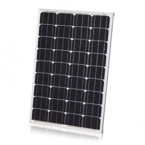
Heterojunction Silicon Wafer Solar Cells Home Lighting Solar Panel Kit 10W to 500W
- Ref Price:
-

- Loading Port:
- China main port
- Payment Terms:
- TT OR LC
- Min Order Qty:
- 500 watt
- Supply Capability:
- 20000000 watt/month
OKorder Service Pledge
OKorder Financial Service
You Might Also Like


Destription:
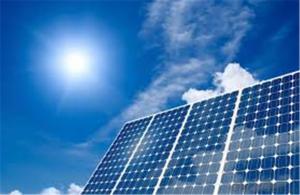
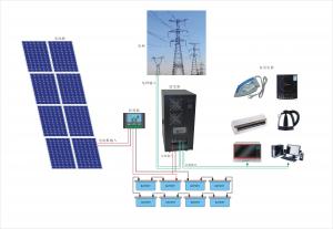
Solar panel refers to a panel designed to absorb the sun's rays as a source of energy for generating electricity or heating. A PV module is a packaged, connected assembly of typically 6×10 solar cells. Solar PV panels constitute the solar array of a photovoltaic system that generates and supplies solar electricity in commercial and residential applications.
Main Characteristic
1.Manufactured according to international quality and Environment Management
System (ISO9001, ISO14001)
2. By the high transmittance, low iron tempered glass, anti-aging of the EVA(polyethylene - vinyl acetate), high-performance crystalline silicon solar cells, good Weather resistance TPT (fluoroplastics composite membrane) by pyramid , has a good Weather resistance and anti-UV, hail, water-proof capacity.
3. OEM and customerized package are accepted
4. High efficiency crystalline silicon solar cells
Quality warranty
1.10 years limited warranty on material and workmanship
2. more than 90% power output in 10 years
3. more than 80% power output in 25 years
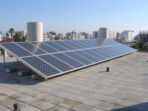
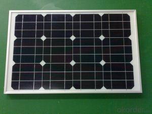
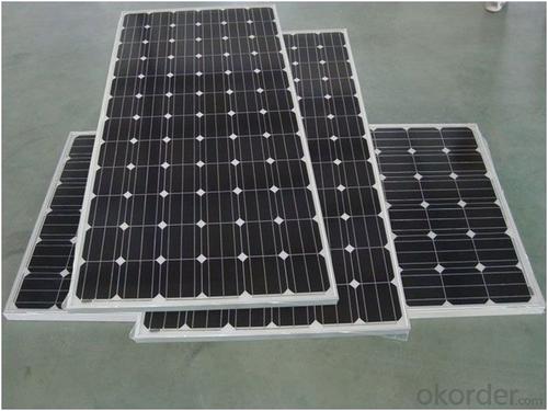
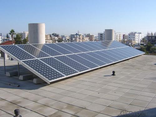
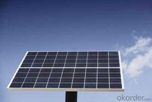
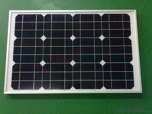
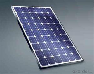
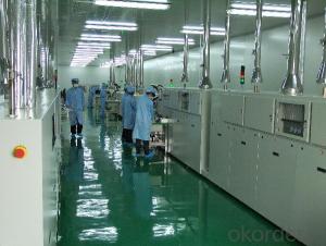
Product show


- Q: Can solar silicon wafers be used in hybrid solar cell technologies?
- Yes, solar silicon wafers can be used in hybrid solar cell technologies. Hybrid solar cells combine different materials, such as silicon and other semiconductors, to enhance their efficiency and performance. By incorporating silicon wafers into hybrid solar cells, their ability to absorb and convert sunlight into electricity can be improved, leading to more efficient solar energy generation.
- Q: What are the properties of a high-quality solar silicon wafer?
- A high-quality solar silicon wafer possesses several key properties. Firstly, it should have a high level of purity, typically above 99.9999%, to ensure minimal impurities that could affect the efficiency of the solar cell. The wafer should also have a uniform crystal structure with low defect density, enabling efficient electron flow and minimizing energy losses. Additionally, a desirable wafer should have a precise thickness, usually around 200 micrometers, to optimize light absorption and minimize material waste. Lastly, a high-quality solar silicon wafer should have a smooth surface with minimal surface roughness, allowing for effective deposition of the solar cell layers and minimizing light reflection.
- Q: What is the impact of crystal orientation on solar silicon wafers?
- The impact of crystal orientation on solar silicon wafers is significant. The orientation of the crystal lattice in the wafer determines its electrical properties and overall efficiency as a solar cell. Different crystal orientations can affect the recombination rate, carrier mobility, and light absorption capabilities of the wafer. For instance, certain orientations like (100) or (111) exhibit higher light absorption, while others may have better charge carrier transport properties. Therefore, optimizing the crystal orientation during the manufacturing process is crucial to enhance the performance and yield of solar silicon wafers.
- Q: How are solar silicon wafers protected from thermal shock during manufacturing?
- Solar silicon wafers are protected from thermal shock during manufacturing through several methods. One common approach is to use thermal annealing, where the wafers are gradually heated and cooled to relieve any internal stress and prevent cracking. Additionally, the use of specialized furnaces and controlled heating processes helps ensure a gradual and uniform temperature change, minimizing the risk of thermal shock. Finally, some manufacturers also apply protective coatings or use support materials to provide extra insulation and buffering against rapid temperature changes, further safeguarding the wafers from thermal shock.
- Q: What are the different types of glass covers used on solar silicon wafers?
- The different types of glass covers used on solar silicon wafers include tempered glass, anti-reflective coated glass, textured glass, and transparent conductive oxide coated glass.
- Q: What is the role of anti-reflective coating on solar silicon wafers?
- The role of anti-reflective coating on solar silicon wafers is to minimize the amount of reflected sunlight, thereby increasing the amount of light that can be absorbed by the solar cells. This coating helps to improve the overall efficiency of the solar panels by allowing more light to pass through and be converted into electricity.
- Q: What is the expected degradation rate of solar silicon wafers over time?
- The expected degradation rate of solar silicon wafers over time varies depending on various factors such as the quality of the silicon material, manufacturing process, environmental conditions, and maintenance practices. However, on average, silicon solar wafers experience a degradation rate of around 0.5-1% per year. This means that after 25 to 30 years, solar panels may have lost around 20-30% of their original efficiency. It's important to note that advancements in technology and improved manufacturing processes are continuously reducing degradation rates, ultimately increasing the lifespan and efficiency of solar panels.
- Q: What is the role of metal contacts on solar silicon wafers?
- The role of metal contacts on solar silicon wafers is to provide electrical connections between the solar cells and external electrical circuitry. These contacts typically act as terminals for the flow of current, allowing the generated electricity to be collected and utilized.
- Q: How do solar silicon wafers perform in desert environments?
- Solar silicon wafers perform well in desert environments due to the abundance of sunlight and high temperatures. The dry climate and low humidity help to optimize the efficiency and output of solar panels made from silicon wafers. However, it is important to consider dust accumulation and periodic cleaning to maintain their performance in such conditions.
- Q: What is the typical thickness tolerance of a solar silicon wafer?
- The typical thickness tolerance of a solar silicon wafer is around 20-30 micrometers.
Send your message to us
Heterojunction Silicon Wafer Solar Cells Home Lighting Solar Panel Kit 10W to 500W
- Ref Price:
-
- Loading Port:
- China main port
- Payment Terms:
- TT OR LC
- Min Order Qty:
- 500 watt
- Supply Capability:
- 20000000 watt/month
OKorder Service Pledge
OKorder Financial Service
Similar products


Hot products


Hot Searches
Related keywords

