
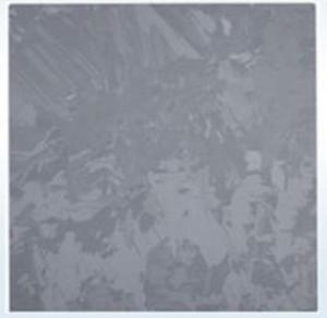


Solar Cell Silicon Wafer - Polycrystalline Solar Silicon Wafer, 125*125mm
- Ref Price:
-

- Loading Port:
- Shanghai Port
- Payment Terms:
- TT or LC
- Min Order Qty:
- 100 Pieces PCS
- Supply Capability:
- 700MW/Per Year PCS/month
OKorder Service Pledge
OKorder Financial Service
You Might Also Like


Specifications of Poly Solar Wafers
|
Product name |
Poly Wafer |
| Conductive type | P Type |
| Square size wafer (mm) | 125×125±0.5 |
| 219.20±0.5 | |
| Corner (mm)
|
1±0.5、45°±10º |
| 200±20 | |
| Total thickness(um) | ≤40 |
| Resistivity ranges(Ωcm) | 1-3 |
| Doping elements | boron |
| Carbon content(atoms/cc) | ≤8*1017 |
| Oxygen content(atoms/cc) | ≤1*1018 |
| Lifetime(μs) | ≥2 |
| Surface quality | No crack, gap, missing Angle, perforated, window, microcrystalline |
| Warping degrees(μm) | ≤50 |
| Neighbouring vertical degree | 90±0.5° |
| Side damage(mm) | ≤0.5mm(length)×0.3mm(width),(not more than 2 per wafer) |
| Line mark(μm) | ≤15 |
Advantages of Poly Solar Wafers
1. High efficiency and High power.
2. Long-term electrical stability.
3. Lowest price and Fastest delivery.
4. Good quality and good service.
5. Bulk supply
6. Good Warranty
7. Big Sale
8. More than 25 years on the lifetime.
Usage and Applications of Poly Solar Wafer
Poly Solar Wafers mainly used to make Poly Solar Cells. Our wafers are your best choice of raw material, which can greatly improve the performance of the Solar Cells and Solar Modules.
Packaging & Delivery of Poly Solar Wafer
Carton Box Package and Deliver by air. It should be noticed that it should be avoid of water, sunshine and moist.
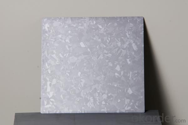
Factory of Solar Wafers

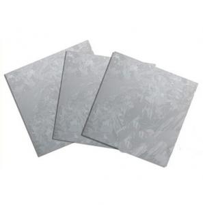
Package Picture of Solar Wafer

- Q: Are solar silicon wafers affected by electromagnetic interference (EMI)?
- Yes, solar silicon wafers can be affected by electromagnetic interference (EMI). EMI refers to the disruption caused by electromagnetic fields on electronic devices, and solar silicon wafers, being electronic components used in solar panels, are not immune to this interference. EMI can potentially impact the efficiency and performance of solar panels, leading to a decrease in power output. Therefore, it is important to consider EMI mitigation techniques during the design and installation of solar systems to minimize its impact on the silicon wafers and overall solar panel performance.
- Q: How is a solar silicon wafer made?
- A solar silicon wafer is made through a series of processes starting with the purification of silicon. The purification involves converting raw silicon into polysilicon, which is then melted and formed into ingots. These ingots are sliced into thin wafers using a wire saw or diamond blade. The wafers are then cleaned, polished, and treated to remove impurities and create a smooth surface. Finally, the wafers undergo various doping processes to enhance their electrical properties and are ready for use in solar cell production.
- Q: What factors contribute to the degradation of a solar silicon wafer?
- Several factors contribute to the degradation of a solar silicon wafer. Firstly, exposure to harsh environmental conditions like extreme temperatures, humidity, and UV radiation can cause the wafer's surface to deteriorate over time. Secondly, impurities present in the silicon material or introduced during the manufacturing process can lead to the formation of defects, reducing the efficiency of the solar cell. Thirdly, mechanical stress, such as thermal expansion or contraction, can cause cracking or warping in the wafer, affecting its performance. Finally, improper handling, installation, or maintenance practices can also contribute to the degradation of a solar silicon wafer.
- Q: Why do you use a concentrated sulfuric acid and hydrogen peroxide to wash silicon?
- Because of the use of sand when the recovery of mortar used too much, resulting in increased viscosity and organic impurities
- Q: What is the role of oxide layers on solar silicon wafers?
- The role of oxide layers on solar silicon wafers is to passivate the surface of the wafer and reduce recombination of charge carriers, thereby improving the efficiency of the solar cell.
- Q: What is the role of interconnection on solar silicon wafers?
- The role of interconnection on solar silicon wafers is to connect individual solar cells together in a series or parallel configuration to form a solar module. This interconnection allows for the flow of electricity generated by the solar cells, enabling the module to produce usable electricity.
- Q: How do solar silicon wafers perform in high-salt environments?
- Solar silicon wafers typically perform well in high-salt environments due to their inherent corrosion resistance. The silicon material used in solar cells is generally resistant to the corrosive effects of saltwater, making it suitable for installations near coastal areas or other high-salt environments. However, it is important to note that other components of the solar panel, such as the frame and electrical connections, may still be susceptible to corrosion and require proper protection measures.
- Q: What is the role of front surface texturing on solar silicon wafers?
- The role of front surface texturing on solar silicon wafers is to increase the absorption of sunlight and improve the overall efficiency of the solar cell. By creating tiny indentations or patterns on the front surface of the wafer, the texturing helps to reduce the reflection of sunlight and increase the chances of light being absorbed by the solar cell. This allows for a higher conversion of sunlight into usable electricity, ultimately increasing the performance and output of the solar panel.
- Q: Are solar silicon wafers affected by dust or dirt accumulation?
- Yes, solar silicon wafers are affected by dust or dirt accumulation. Dust and dirt can block sunlight from reaching the surface of the wafers, reducing their efficiency and power output. Regular cleaning and maintenance are necessary to ensure optimal performance of solar panels.
- Q: What is the purpose of a temperature coefficient in a solar silicon wafer?
- The purpose of a temperature coefficient in a solar silicon wafer is to quantify how the performance and efficiency of the solar cell are affected by changes in temperature. It allows us to understand and account for the variations in electrical output that occur as the temperature of the solar cell changes, helping in the accurate prediction and optimization of solar cell performance under different temperature conditions.
1. Manufacturer Overview
| Location | |
| Year Established | |
| Annual Output Value | |
| Main Markets | |
| Company Certifications |
2. Manufacturer Certificates
| a) Certification Name | |
| Range | |
| Reference | |
| Validity Period |
3. Manufacturer Capability
| a) Trade Capacity | |
| Nearest Port | |
| Export Percentage | |
| No.of Employees in Trade Department | |
| Language Spoken: | |
| b) Factory Information | |
| Factory Size: | |
| No. of Production Lines | |
| Contract Manufacturing | |
| Product Price Range | |
Send your message to us
Solar Cell Silicon Wafer - Polycrystalline Solar Silicon Wafer, 125*125mm
- Ref Price:
-
- Loading Port:
- Shanghai Port
- Payment Terms:
- TT or LC
- Min Order Qty:
- 100 Pieces PCS
- Supply Capability:
- 700MW/Per Year PCS/month
OKorder Service Pledge
OKorder Financial Service
Similar products


Hot products


Hot Searches

