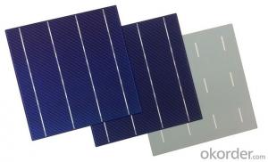
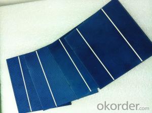
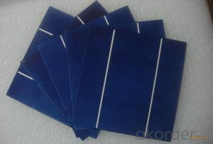
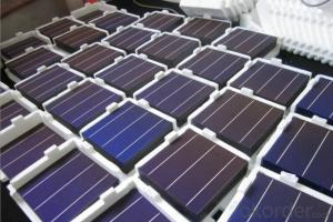
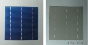
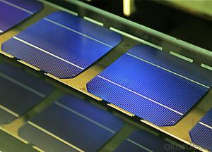
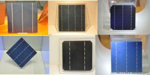
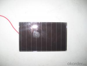
Silicon Wafer Solar - High Quality A Grade Polycrystalline 5V 16.2% Solar Cell
- Loading Port:
- Shanghai
- Payment Terms:
- TT OR LC
- Min Order Qty:
- 1000 pc
- Supply Capability:
- 100000 pc/month
OKorder Service Pledge
OKorder Financial Service
You Might Also Like
Specifications
hot sale solar cell
1.16.8%~18.25% high efficiency
2.100% checked quality
3.ISO9001/ISO14001/TUV/CE/UL
4.stable performance
We can offer you the best quality products and services, don't miss !
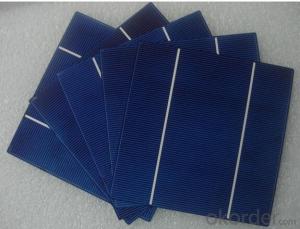
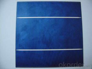
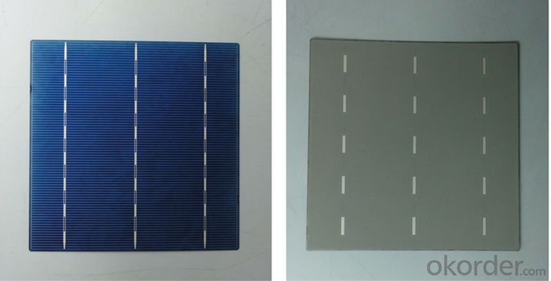
POLY6'(156*156)
Polycrystalline Silicon Solar cell
Physical Characteristics
Dimension: 156mm×156mm±0.5mm
Diagonal: 220mm±0.5mm
Thickness(Si): 200±20 μm
Front(-) Back(+)
Blue anti-reflecting coating (silicon nitride); Aluminum back surface field;
1.5mm wide bus bars; 2.0mm wide soldering pads;
Distance between bus bars: 51mm . Distance between bus bars :51mm .
Electrical Characteristics
Efficiency(%) | 18.00 | 17.80 | 17.60 | 17.40 | 17.20 | 16.80 | 16.60 | 16.40 | 16.20 | 16.00 | 15.80 | 15.60 |
Pmpp(W) | 4.33 | 4.29 | 4.24 | 4.19 | 4.14 | 4.09 | 4.04 | 3.99 | 3.94 | 3.90 | 3.86 | 3.82 |
Umpp(V) | 0.530 | 0.527 | 0.524 | 0.521 | 0.518 | 0.516 | 0.514 | 0.511 | 0.509 | 0.506 | 0.503 | 0.501 |
Impp(A) | 8.159 | 8.126 | 8.081 | 8.035 | 7.990 | 7.938 | 7.876 | 7.813 | 7.754 | 7.698 | 7.642 | 7.586 |
Uoc(V) | 0.633 | 0.631 | 0.628 | 0.625 | 0.623 | 0.620 | 0.618 | 0.617 | 0.615 | 0.613 | 0.611 | 0.609 |
Isc(A) | 8.709 | 8.677 | 8.629 | 8.578 | 8.531 | 8.478 | 8.419 | 8.356 | 8.289 | 8.220 | 8.151 | 8.083 |
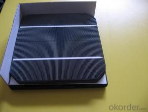
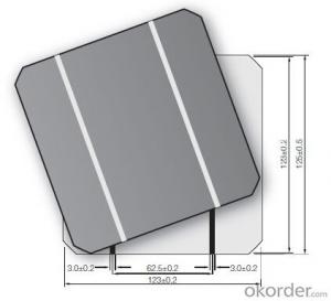
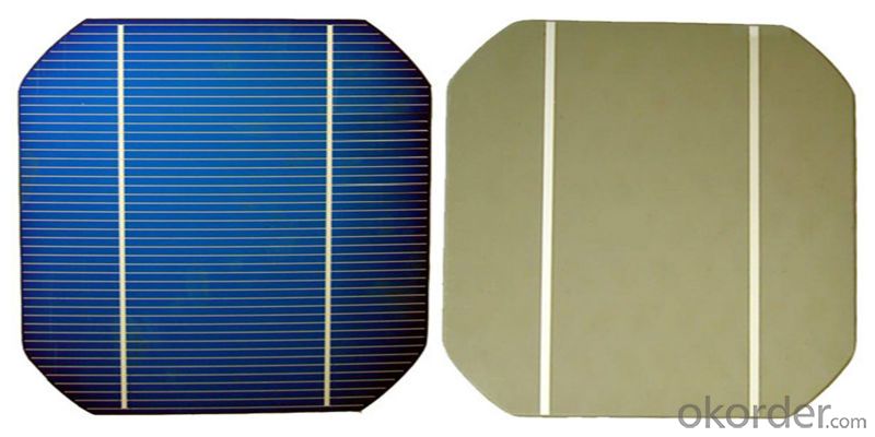
MONO5'(125*125mm)165
Monocrystalline silicon solar cell
Physical Characteristics
Dimension: 125mm×125mm±0.5mm
Diagonal: 165mm±0.5mm
Thickness(Si): 200±20 μm
Front(-) Back(+)
Blue anti-reflecting coating(silicon nitride); Aluminum back surface field;
1.6mmwide bus bars; 2.5mm wide soldering pads;
Distance between bus bars: 61mm . Distance between bus bars :61mm .
Electrical Characteristics
Efficiency(%) | 19.40 | 19.20 | 19.00 | 18.80 | 18.60 | 18.40 | 18.20 | 18.00 | 17.80 | 17.60 | 17.40 | 17.20 |
Pmpp(W) | 2.97 | 2.94 | 2.91 | 2.88 | 2.85 | 2.82 | 2.79 | 2.76 | 2.73 | 2.70 | 2.67 | 2.62 |
Umpp(V) | 0.537 | 0.535 | 0.533 | 0.531 | 0.527 | 0.524 | 0.521 | 0.518 | 0.516 | 0.515 | 0.513 | 0.509 |
Impp(A) | 5.531 | 5.495 | 5.460 | 5.424 | 5.408 | 5.382 | 5.355 | 5.328 | 5.291 | 5.243 | 5.195 | 4.147 |
Uoc(V) | 0.637 | 0.637 | 0.636 | 0.635 | 0.633 | 0.630 | 0.629 | 0.629 | 0.628 | 0.626 | 0.626 | 0.625 |
Isc(A) | 5.888 | 5.876 | 5.862 | 5.848 | 5.839 | 5.826 | 5.809 | 5.791 | 5.779 | 5.756 | 5.293 | 5.144 |
FAQ:
Q:How can i get some sample?
A:Yes , if you want order ,sample is not a problem.
Q:How about your solar panel efficency?
A: Our product efficency around 17.25%~18.25%.
Q:What’s the certificate you have got?
A: we have overall product certificate of ISO9001/ISO14001/CE/TUV/UL
- Q: What are the different doping materials used in solar silicon wafers?
- The different doping materials used in solar silicon wafers include phosphorus and boron. Phosphorus is used as a donor material to create n-type silicon wafers, while boron is used as an acceptor material to create p-type silicon wafers. These doping materials help to create the necessary electrical properties within the silicon wafers, allowing them to efficiently convert sunlight into electricity.
- Q: What is the purpose of a grounding wire in a solar silicon wafer?
- The purpose of a grounding wire in a solar silicon wafer is to provide a safe path for electrical current to flow in case of a fault or malfunction. This helps to protect the equipment and prevent electrical shocks or damage.
- Q: How is a glass cover attached to a solar silicon wafer?
- A glass cover is typically attached to a solar silicon wafer using an adhesive material or a combination of adhesive and pressure. The adhesive is applied to the edges of the wafer, and then the glass cover is carefully placed on top, ensuring a proper alignment and bonding. This attachment provides protection to the wafer and helps in maintaining its structural integrity and efficiency.
- Q: What is the size of a typical solar silicon wafer?
- A typical solar silicon wafer is typically 156 mm (6.14 inches) in size.
- Q: How are solar silicon wafers affected by light-induced annealing?
- Solar silicon wafers are positively affected by light-induced annealing. This process helps to reduce defects and improve the overall efficiency of the wafers by repairing crystal lattice damage caused during fabrication.
- Q: Are all solar panels made with silicon wafers?
- No, not all solar panels are made with silicon wafers. While silicon is the most commonly used material for solar panels, there are also other types of solar panels available such as thin-film solar panels that utilize different materials like cadmium telluride or copper indium gallium selenide.
- Q: What is the purpose of a junction box in a solar silicon wafer?
- The purpose of a junction box in a solar silicon wafer is to provide a secure and protective enclosure for the electrical connections between the solar cells and the external electrical system. It helps to ensure the safety and reliability of the solar panel by protecting the wiring and connections from environmental factors such as moisture, dust, and heat. Additionally, the junction box allows for easy access to the electrical connections for maintenance and troubleshooting purposes.
- Q: What is the role of an interconnect in a solar silicon wafer?
- The role of an interconnect in a solar silicon wafer is to establish electrical connections between individual solar cells within the wafer. These interconnects help in efficiently transferring the generated electricity from the solar cells to the external circuitry, enabling the conversion of sunlight into usable electrical energy.
- Q: What specific steps should be used to clean the wafer? A little more detail
- LED (Light Emitting Diode), light emitting diode, referred to as LED, is a kind of power can be converted into visible light solid-state semiconductor devices, which can directly convert electricity into light. The heart of LED is a semiconductor chip, one end of which is attached to a support, one end is a negative electrode, and the other end is connected with the positive electrode of the power supply so that the whole chip is encapsulated by epoxy resin. The semiconductor chip is made up of two parts, one part is the P type semiconductor, in which the hole is dominant, the other end is the N type semiconductor.
- Q: What is the role of solar silicon wafers in promoting energy independence at the community level?
- Solar silicon wafers play a crucial role in promoting energy independence at the community level. These wafers are the key component in solar panels, which convert sunlight into electricity. By harnessing solar power, communities can reduce their reliance on traditional fossil fuel sources, contributing to a greener and more sustainable energy future. Solar silicon wafers enable the generation of clean and renewable energy, reducing carbon emissions and dependence on external energy providers. This helps communities become self-sufficient in meeting their energy needs, leading to greater energy independence and resilience.
Send your message to us
Silicon Wafer Solar - High Quality A Grade Polycrystalline 5V 16.2% Solar Cell
- Loading Port:
- Shanghai
- Payment Terms:
- TT OR LC
- Min Order Qty:
- 1000 pc
- Supply Capability:
- 100000 pc/month
OKorder Service Pledge
OKorder Financial Service
Similar products
Hot products
Hot Searches
Related keywords
