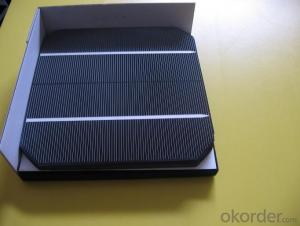
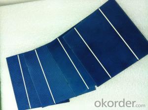
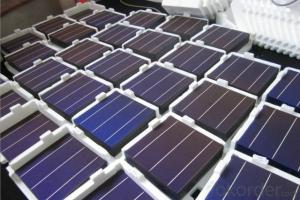
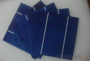
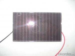
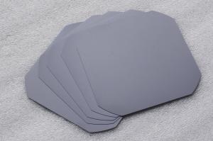
Heterojunction Silicon Wafer Solar Cells - High Quality A Grade Polycrystalline 5V 15.6% Solar Cell
- Loading Port:
- Shanghai
- Payment Terms:
- TT OR LC
- Min Order Qty:
- 1000 pc
- Supply Capability:
- 100000 pc/month
OKorder Service Pledge
OKorder Financial Service
You Might Also Like
Specifications
hot sale solar cell
1.16.8%~18.25% high efficiency
2.100% checked quality
3.ISO9001/ISO14001/TUV/CE/UL
4.stable performance
We can offer you the best quality products and services, don't miss !
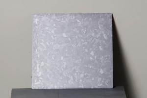
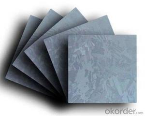
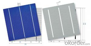
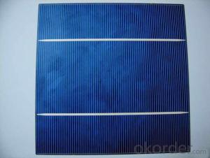
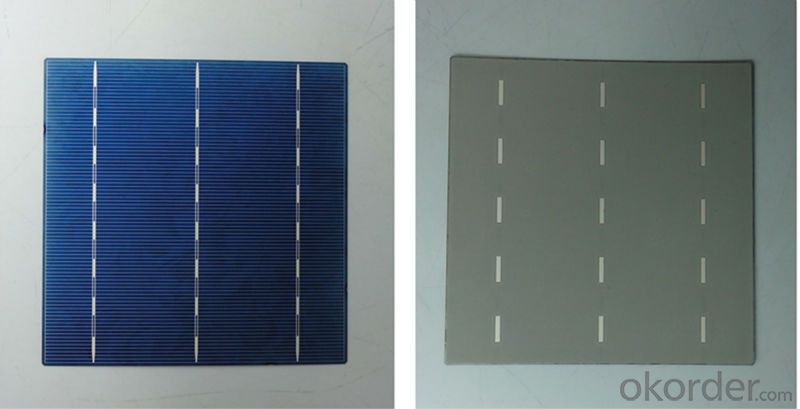
POLY6'(156*156)
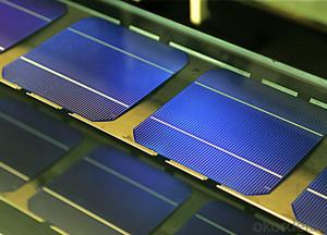
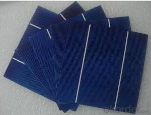
Polycrystalline Silicon Solar cell
Physical Characteristics
Dimension: 156mm×156mm±0.5mm
Diagonal: 220mm±0.5mm
Thickness(Si): 200±20 μm
Front(-) Back(+)
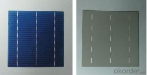
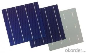
Blue anti-reflecting coating (silicon nitride); Aluminum back surface field;
1.5mm wide bus bars; 2.0mm wide soldering pads;
Distance between bus bars: 51mm . Distance between bus bars :51mm .
Electrical Characteristics
Efficiency(%) | 18.00 | 17.80 | 17.60 | 17.40 | 17.20 | 16.80 | 16.60 | 16.40 | 16.20 | 16.00 | 15.80 | 15.60 |
Pmpp(W) | 4.33 | 4.29 | 4.24 | 4.19 | 4.14 | 4.09 | 4.04 | 3.99 | 3.94 | 3.90 | 3.86 | 3.82 |
Umpp(V) | 0.530 | 0.527 | 0.524 | 0.521 | 0.518 | 0.516 | 0.514 | 0.511 | 0.509 | 0.506 | 0.503 | 0.501 |
Impp(A) | 8.159 | 8.126 | 8.081 | 8.035 | 7.990 | 7.938 | 7.876 | 7.813 | 7.754 | 7.698 | 7.642 | 7.586 |
Uoc(V) | 0.633 | 0.631 | 0.628 | 0.625 | 0.623 | 0.620 | 0.618 | 0.617 | 0.615 | 0.613 | 0.611 | 0.609 |
Isc(A) | 8.709 | 8.677 | 8.629 | 8.578 | 8.531 | 8.478 | 8.419 | 8.356 | 8.289 | 8.220 | 8.151 | 8.083 |
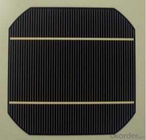
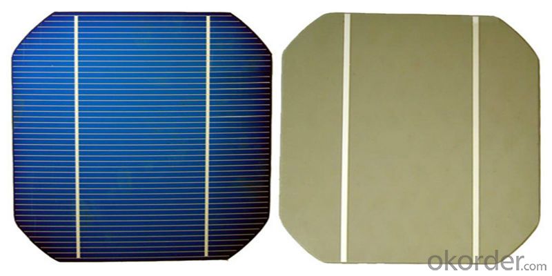
MONO5'(125*125mm)165
Monocrystalline silicon solar cell
Physical Characteristics
Dimension: 125mm×125mm±0.5mm
Diagonal: 165mm±0.5mm
Thickness(Si): 200±20 μm
Front(-) Back(+)
Blue anti-reflecting coating(silicon nitride); Aluminum back surface field;
1.6mmwide bus bars; 2.5mm wide soldering pads;
Distance between bus bars: 61mm . Distance between bus bars :61mm .
Electrical Characteristics
Efficiency(%) | 19.40 | 19.20 | 19.00 | 18.80 | 18.60 | 18.40 | 18.20 | 18.00 | 17.80 | 17.60 | 17.40 | 17.20 |
Pmpp(W) | 2.97 | 2.94 | 2.91 | 2.88 | 2.85 | 2.82 | 2.79 | 2.76 | 2.73 | 2.70 | 2.67 | 2.62 |
Umpp(V) | 0.537 | 0.535 | 0.533 | 0.531 | 0.527 | 0.524 | 0.521 | 0.518 | 0.516 | 0.515 | 0.513 | 0.509 |
Impp(A) | 5.531 | 5.495 | 5.460 | 5.424 | 5.408 | 5.382 | 5.355 | 5.328 | 5.291 | 5.243 | 5.195 | 4.147 |
Uoc(V) | 0.637 | 0.637 | 0.636 | 0.635 | 0.633 | 0.630 | 0.629 | 0.629 | 0.628 | 0.626 | 0.626 | 0.625 |
Isc(A) | 5.888 | 5.876 | 5.862 | 5.848 | 5.839 | 5.826 | 5.809 | 5.791 | 5.779 | 5.756 | 5.293 | 5.144 |
FAQ:
Q:How can i get some sample?
A:Yes , if you want order ,sample is not a problem.
Q:How about your solar panel efficency?
A: Our product efficency around 17.25%~18.25%.
Q:What’s the certificate you have got?
A: we have overall product certificate of ISO9001/ISO14001/CE/TUV/UL
- Q: Can solar silicon wafers be used in off-grid applications?
- Yes, solar silicon wafers can be used in off-grid applications. Off-grid applications refer to systems or devices that are not connected to the main electrical grid and rely on alternative sources of power. Solar silicon wafers, when used in conjunction with other components such as solar cells, can capture sunlight and convert it into electricity, making them an ideal choice for generating power in off-grid scenarios.
- Q: What is the expected future development of solar silicon wafers?
- The expected future development of solar silicon wafers is likely to focus on enhancing their efficiency, reducing production costs, and improving their durability. Technological advancements may include the development of high-efficiency wafers, such as tandem or multi-junction cells, which can capture a wider range of sunlight and convert it into electricity more effectively. Additionally, innovations in manufacturing processes, such as thinner wafers and new deposition techniques, may help reduce costs and increase production yields. Furthermore, efforts to enhance the durability of solar silicon wafers, making them more resistant to degradation and longer-lasting, will be crucial to ensure their long-term performance and economic viability.
- Q: What is a silicon chip made of?
- A simple understanding of the silicon wafer is a silicon material cut into pieces by processing. Silicon is a kind of high hardness material, silicon material looks like a stone, he must be washed clean and then heated by a stove melt forming a bulk silicon ingot, and then use the special machine to slice into pieces.
- Q: Wafer size6 inches and 8 inches only refers to the diameter of monocrystalline silicon?Recently heard that the polysilicon film also has 6 inches and 8 inches, 6 inches of polysilicon is 125mm*125mm square, which is 8 inches 156mm*156mm 6 inches, but the conversion is 150.2mm, there is nothing like 125mm, if 6 inches is diagonal, the square of the 125mm wafer diagonal length 176.75mm also, not 6 inches?In addition, the 8 inch silicon wafer size also has similar doubts, to solve the.Thanks!
- Refers to the diagonal length of the silicon waferBut you asked the wrong question, the wafer is divided into monocrystalline silicon and polycrystalline silicon wafer, you say is a square of silicon polysilicon film of silicon wafer, you ask in the four corner is a circular arc shape, so you should also count the length of the diagonal right. If not to shape the polysilicon film solution you can search the Internet search look.
- Q: Why do monocrystalline silicon chamfer? Polysilicon film?
- There are many single crystal chamfer.Single crystals are generally large chamfer, there is a single crystal process decision. There is a single crystal silicon rod is cut out, in order to make full use of the silicon rod, appear large chamfer; and polycrystalline is generally small chamfer, is to reduce the crack edge of the silicon wafer, the external stress of the silicon wafer or cell rupture. Polycrystalline battery will also appear large chamfer, those are generally small chamfer of the battery, found that there is a problem after the cut into large chamfer.
- Q: What is the difference between monocrystalline and polycrystalline silicon wafers?
- The main difference between monocrystalline and polycrystalline silicon wafers lies in their crystal structure. Monocrystalline silicon wafers are made from a single crystal structure, resulting in a uniform and continuous crystal lattice. On the other hand, polycrystalline silicon wafers are made from multiple smaller crystals, which leads to a less uniform and discontinuous crystal structure. This difference in structure affects the efficiency and performance of solar cells made from these wafers, with monocrystalline wafers generally offering higher efficiency but at a higher cost, while polycrystalline wafers provide a more cost-effective option with slightly lower efficiency.
- Q: How does the efficiency of a solar silicon wafer change with wind speed?
- The efficiency of a solar silicon wafer is not directly affected by wind speed. Wind speed does not have a significant impact on the performance or efficiency of a solar silicon wafer as long as it is securely mounted and protected from any potential damage caused by high winds.
- Q: What is the role of back surface field in solar silicon wafers?
- The role of the back surface field in solar silicon wafers is to enhance the efficiency of the solar cell by reducing recombination and increasing the collection of charge carriers generated by sunlight. It creates a strong electric field at the back surface of the wafer, pushing the minority carriers towards the front surface, where they can be collected and harnessed to generate electricity.
- Q: How does the cost of a solar silicon wafer compare to other types of solar cells?
- The cost of a solar silicon wafer is generally higher compared to other types of solar cells. While silicon wafers are the most widely used and efficient form of solar cells, they require complex manufacturing processes and the use of high-quality silicon materials, contributing to their higher cost. Other types of solar cells, such as thin-film solar cells, may have lower production costs, but they often sacrifice efficiency and durability. Overall, although silicon wafers are more expensive, their superior performance and longer lifespan make them a preferred choice for many solar applications.
- Q: Can solar silicon wafers be repaired if damaged?
- No, solar silicon wafers cannot be repaired once they are damaged.
Send your message to us
Heterojunction Silicon Wafer Solar Cells - High Quality A Grade Polycrystalline 5V 15.6% Solar Cell
- Loading Port:
- Shanghai
- Payment Terms:
- TT OR LC
- Min Order Qty:
- 1000 pc
- Supply Capability:
- 100000 pc/month
OKorder Service Pledge
OKorder Financial Service
Similar products
Hot products
Hot Searches
Related keywords
