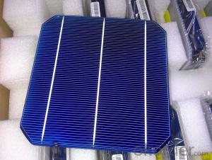


Mono Solar Cells156mm*156mm in Bulk Quantity Low Price Stock 19.4
- Ref Price:
-

- Loading Port:
- Shanghai
- Payment Terms:
- TT OR LC
- Min Order Qty:
- 1000 pc
- Supply Capability:
- 100000 pc/month
OKorder Service Pledge
OKorder Financial Service
You Might Also Like


Brief Introduction
- Up to 20.0% efficiency, one of the highest performing mono crystalline cells on the market
- Three bus bars boosts current collection over the entire cell area, leading to higher fill factors
- Blue anti-reflecting coating allows more sunlight be captured and converted to electricity
- Finer, closer fingers improves charge collections for improved energy yield
- Lower light-induced degradation leads to greater power output over the entire module lifetime
- All solar cells are tightly classified to optimize output of module
- Maximum yield and longevity due to hotspot prevention
- Premium appearance results in a highly uniform and aesthetically appealing module
Specification
- Product Mono-crystalline silicon solar cell
- Dimension 156 mm x 156 mm ± 0.5 mm
- Thickness 200 μm ± 30 μm
- Front 1.5 ± 0.1 mm busbar (silver)
- Silicon nitride antireflection coating
- Back 3.0 mm continuous soldering pads (silver)
- Back surface field (aluminum)
Electric performance parameters

- Testing conditions: 1000 W/m2, AM 1.5, 25 °C, Tolerance: Efficiency ± 0.2% abs., Pmpp ±1.5% rel.
- Imin : at 0.5 V
Light Intensity Dependence

Soldering Ability
- Peel Strength: > 1.0 N/mm (Pull soldered ribbon from busbar in 5 mm/s of 180°)
Dimension Figure

Quick Response
- Any time and anywhere, reply clients' email and solve all problems happen in the work at the first time.
- Remove clients doubts and offer the best solution at the first time.
- Give our clients the lastest news of the photovoltaic, update the newest stock informtion.
Production and Quality Control
- Precision cell efficiency sorting procedures
- Stringent criteria for color uniformity and appearance
- Reverse current and shunt resistance screening
- ISO9001,ISO14001 and OHSAS 18001,TUV Certificated


FAQ:
1. Q: Do you have your own factory?
A: Yes, we have. Our factory located in Jiangsu
2. Q: How can I visit your factory?
A: Before you visit,please contact us.We will show you the route or arrange a car to pick you up.
3. Q: Do you provide free sample?
A: Commenly we provide paid sample.
4. Q: Could you print our company LOGO on the nameplate and package?
A: Yes, we accept it.And need an Authorization Letter from you.
5. Q: Do you accept custom design on size?
A: Yes, if the size is reasonable.
6. Q: How can I be your agent in my country?
A: Please leave feedback. It's better for us to talk about details by email.
7. Q: Do you have solar project engineer who can guide me to install system?
A: Yes, we have a professional engineer team. They can teach you how to install a solar system.
- Q:Are solar silicon wafers affected by vibrations or shocks?
- Yes, solar silicon wafers can be affected by vibrations or shocks. Vibrations or shocks can cause microcracks or fractures in the wafers, which can lead to reduced efficiency or even complete failure of the solar cells. Therefore, it is important to handle and transport solar silicon wafers with care to avoid any damage from vibrations or shocks.
- Q:How are solar silicon wafers protected from moisture during storage?
- Solar silicon wafers are typically protected from moisture during storage by being sealed in airtight containers or packaging materials that have low moisture permeability. This prevents any moisture from coming in contact with the wafers, which could potentially degrade their performance or cause damage. Additionally, desiccant packets or moisture-absorbing materials are commonly used inside the packaging to further minimize moisture levels and maintain the integrity of the wafers.
- Q:What is the purpose of a backsheet in a solar silicon wafer?
- The purpose of a backsheet in a solar silicon wafer is to protect the solar cells from external elements such as moisture, dust, and UV radiation. It acts as a barrier, preventing any damage or degradation to the solar cells, thus ensuring their longevity and optimal performance. Additionally, the backsheet also provides electrical insulation and improves the overall efficiency of the solar panel by reflecting any excess light back onto the solar cells.
- Q:How do solar silicon wafers perform in areas with high air pollution?
- Solar silicon wafers are generally not affected by high air pollution in terms of their performance. The efficiency and functionality of solar silicon wafers primarily depend on the amount of sunlight they receive rather than the air quality. However, it is worth noting that the accumulation of dust and particles on the surface of the wafers can reduce their overall efficiency. Regular cleaning or maintenance might be required to ensure optimal performance in areas with high air pollution.
- Q:Can solar silicon wafers be used in recreational vehicles (RVs)?
- Yes, solar silicon wafers can be used in recreational vehicles (RVs). Solar panels made with silicon wafers are commonly used in RVs to harness solar energy and provide power for various appliances and systems while on the road or camping.
- Q:Process flow of wafer wafer ultrasonic cleaning machine?
- Solar silicon wafer surface plasma cleaning processResidual plasma cleaning method of particles on silicon wafer surface, which comprises the following steps: firstly, gas flushing process, and then the gas plasma glow. The plasma cleaning method for removing particles of silicon surface easy control, thorough cleaning, no residual reactants, the process gas, non-toxic, low cost, small amount of labor, work efficiency high.
- Q:How do solar silicon wafers contribute to energy storage systems?
- Solar silicon wafers are an essential component of energy storage systems as they serve as the foundation for solar panels. These wafers are made from highly pure silicon, allowing them to efficiently convert sunlight into electricity through the photovoltaic effect. By harnessing solar energy and converting it into electrical energy, solar silicon wafers enable the generation of clean and renewable power. This electricity can then be stored in batteries or other energy storage systems, ensuring a continuous supply of eco-friendly energy even when the sun is not shining.
- Q:How are solar silicon wafers interconnected to form solar modules?
- Solar silicon wafers are interconnected to form solar modules through a process called stringing and tabbing. This involves soldering thin metal strips called busbars onto the front and back surfaces of the wafers, creating electrical connections. The busbars serve as positive and negative terminals, allowing the flow of electricity between the cells. Multiple interconnected cells are then encapsulated in a protective layer, such as glass or polymer, to form a complete solar module.
- Q:How are solar silicon wafers affected by thermal annealing?
- Solar silicon wafers are positively affected by thermal annealing. This process helps in reducing defects and impurities present in the silicon material by enhancing crystal structure and improving carrier mobility. Additionally, thermal annealing ensures better electrical conductivity and overall efficiency of the solar cells made from these wafers.
- Q:How are solar silicon wafers connected to form a solar panel?
- Solar silicon wafers are connected to form a solar panel by aligning and soldering them together, usually in a grid-like pattern. These wafers are typically connected with thin metal strips called busbars, which allow the current to flow between the individual cells and create an electrical circuit. The interconnected wafers are then encapsulated in a protective layer, such as tempered glass or a polymer, to ensure durability and efficient performance.
1. Manufacturer Overview |
|
|---|---|
| Location | |
| Year Established | |
| Annual Output Value | |
| Main Markets | |
| Company Certifications | |
2. Manufacturer Certificates |
|
|---|---|
| a) Certification Name | |
| Range | |
| Reference | |
| Validity Period | |
3. Manufacturer Capability |
|
|---|---|
| a)Trade Capacity | |
| Nearest Port | |
| Export Percentage | |
| No.of Employees in Trade Department | |
| Language Spoken: | |
| b)Factory Information | |
| Factory Size: | |
| No. of Production Lines | |
| Contract Manufacturing | |
| Product Price Range | |
Send your message to us
Mono Solar Cells156mm*156mm in Bulk Quantity Low Price Stock 19.4
- Ref Price:
-
- Loading Port:
- Shanghai
- Payment Terms:
- TT OR LC
- Min Order Qty:
- 1000 pc
- Supply Capability:
- 100000 pc/month
OKorder Service Pledge
OKorder Financial Service
Similar products


New products
Hot products


Hot Searches
Related keywords

