


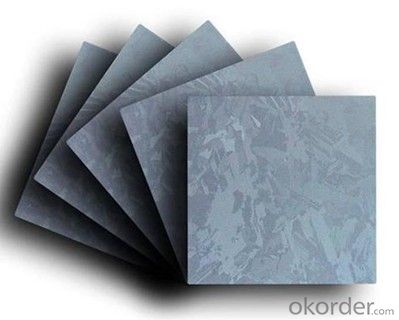

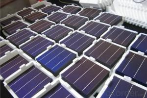
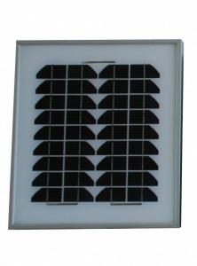
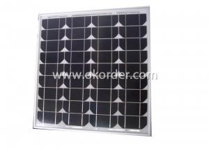
Solar Silicon Wafer
- Ref Price:
-

- Loading Port:
- China Main Port
- Payment Terms:
- TT OR LC
- Min Order Qty:
- -
- Supply Capability:
- -
OKorder Service Pledge
Quality Product, Order Online Tracking, Timely Delivery
OKorder Financial Service
Credit Rating, Credit Services, Credit Purchasing
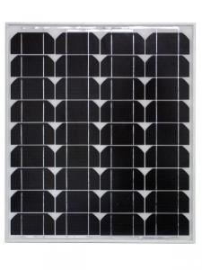
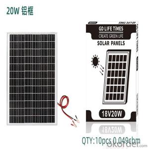
You Might Also Like


Specifications
IC grade mono silicon wafer
1.Used in various discrete devices
2.High Purity 11N
3.Growth Method :CZ
![]()
| IC grade mono silicon wafer | ||
| Size | 4"/5"/6" | |
| Growth method | CZ | |
| Grade | Prime grade | |
| Diameter | 100±0.4mm / 125±0.5mm / 150±0.5mm | |
| Orientation | <111>/<100> | |
| Type | N-type/P-type | |
| Dopant | P-type:Boron | |
| N-type:Phos./As./Sb. | ||
| Purity | 11N(99.999999999%) | |
| Oxygen Content | ≤18 New PPMA | |
| Carborn Content | ≤1 New PPMA | |
| Resistivity | ≥0.001Ω·cm | |
| Thickness | ≥200um, or according to your requirement | |
| Others | TTV≤10um, Bow≤35um,Warp≤35um | |
| Particles | ≥0.3um@≤10PPW | |
| Surface | Frond side polished,back side etched. | |
| MOQ | 100pcs | |
| Package | Packed in cassette,and sealed in vacuum bag,25pcs/cassette. | |
| Price | According to your specification,especially resistivity and thickness | |


- Q:Are solar silicon wafers affected by electromagnetic waves?
- Yes, solar silicon wafers can be affected by electromagnetic waves. Electromagnetic waves can induce currents within the silicon material, causing interference and reducing the efficiency of solar panels. However, solar panels are designed to minimize these effects and are often shielded to mitigate electromagnetic interference.
- Q:What are the main differences between monocrystalline and polycrystalline solar silicon wafers?
- The main differences between monocrystalline and polycrystalline solar silicon wafers lie in their fabrication process and efficiency. Monocrystalline wafers are made from a single crystal structure, resulting in a uniform and pure composition. This allows them to have higher efficiency and power output, making them more suitable for applications with limited space. On the other hand, polycrystalline wafers are made from multiple crystal structures, which leads to lower efficiency and slightly lower power output. However, they are less expensive to produce and can still be effective in larger installations where space is not a constraint.
- Q:Solar silicon wafer cutting fluid content is polyethylene glycol, flash point 182-278 DEG C, saturated vapor pressure of 6.21KPa/20 C / C in storage in the barrel, after exposure, its volatile gas is harmful?
- Silicon in a weak base and water will slowly release hydrogen
- Q:What are the different materials used for passivation layers in solar silicon wafers?
- The different materials used for passivation layers in solar silicon wafers include silicon nitride (SiNx), aluminum oxide (Al2O3), and silicon oxide (SiOx). These materials help reduce surface recombination and enhance the efficiency of solar cells by preventing unwanted carrier losses.
- Q:What is the purity level of the silicon used in solar silicon wafers?
- The purity level of the silicon used in solar silicon wafers is typically very high, with a purity level of 99.9999% (6N) or even higher.
- Q:How are solar silicon wafers packaged and shipped?
- Solar silicon wafers are typically packaged and shipped in protective containers or trays. These containers are designed to securely hold the wafers in place and protect them from damage during transportation. The wafers are carefully stacked in the packaging with appropriate spacing to prevent any contact or scratching. Additionally, the packaging may include layers of foam or other cushioning materials to provide further protection. Once packaged, the wafers are typically shipped in bulk using suitable shipping methods, such as air freight or specialized carriers, to ensure safe delivery to their destination.
- Q:How to make monocrystalline silicon solar panels? Begged: specific steps
- Surface fleeceThe preparation of single crystal silicon wafer is the use of anisotropic etching of silicon on the surface of the silicon per square centimeter to form several million square pyramidal structure, namely, the Pyramid structure. Due to the multiple reflection and refraction of incident light on the surface, the absorption of light is increased, and the short circuit current and conversion efficiency are improved. Anisotropic etching of silicon in alkaline solution liquid is usually hot, available alkali sodium hydroxide, potassium hydroxide, lithium hydroxide and ethylenediamine etc.. Most of them were prepared by using dilute sodium hydroxide solution with a concentration of about 1%, and the corrosion temperature was 70-85. In order to obtain a uniform texture, but also in the solution add alcohols such as ethanol and isopropanol as complexing agent to accelerate the corrosion of silicon. In the preparation of velvet, the silicon chip must be first surface corrosion, alkaline or acidic etching solution to about 20 ~ 25 m, corrosion in the face, the general chemical cleaning. After surface preparation of silicon wafers are not suitable for long-term storage in the water, in order to prevent contamination, should be spread as soon as possible.
- Q:What is the expected growth rate for the solar silicon wafer market?
- The expected growth rate for the solar silicon wafer market is projected to be significant, with estimates suggesting an annual growth rate of around 6% to 8% over the next few years. This growth is driven by the increasing adoption of solar energy, the push for clean and renewable sources of power, and advancements in solar technology.
- Q:Consult the difference between silicon and battery
- Silicon wafer is generally refers to the silicon ingot with diamond wire or just cut into pieces,
- Q:How is a tracker integrated into a solar silicon wafer?
- A tracker is not integrated into a solar silicon wafer. A tracker is a separate component used in solar panel systems to maximize their energy generation by adjusting the angle and direction of the panels based on the movement of the sun. The silicon wafer, on the other hand, is the main component of a solar cell that converts sunlight into electricity.
1. Manufacturer Overview |
|
|---|---|
| Location | |
| Year Established | |
| Annual Output Value | |
| Main Markets | |
| Company Certifications | |
2. Manufacturer Certificates |
|
|---|---|
| a) Certification Name | |
| Range | |
| Reference | |
| Validity Period | |
3. Manufacturer Capability |
|
|---|---|
| a)Trade Capacity | |
| Nearest Port | |
| Export Percentage | |
| No.of Employees in Trade Department | |
| Language Spoken: | |
| b)Factory Information | |
| Factory Size: | |
| No. of Production Lines | |
| Contract Manufacturing | |
| Product Price Range | |
Send your message to us
Solar Silicon Wafer
- Ref Price:
-
- Loading Port:
- China Main Port
- Payment Terms:
- TT OR LC
- Min Order Qty:
- -
- Supply Capability:
- -
OKorder Service Pledge
Quality Product, Order Online Tracking, Timely Delivery
OKorder Financial Service
Credit Rating, Credit Services, Credit Purchasing
Similar products


New products
Hot products


Hot Searches

