


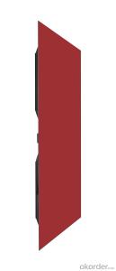
156*156mm 3BB Mono-crystalline Silicon Solar Cell
- Ref Price:
-

- Loading Port:
- China main port
- Payment Terms:
- TT OR LC
- Min Order Qty:
- 100 watt
- Supply Capability:
- 10000 watt/month
OKorder Service Pledge
OKorder Financial Service
You Might Also Like


156*156mm 3BB Mono-crystalline Silicon Solar Cell
Solar Module Summarize
Solar Module is the core part of solar PV power systems,also is the highest value part of it. The function of Solor Module is to convert the sun's radiation to electrical energy, or transfer it to battery and store in it, or to drive the load running.
The Product has been widely used in space and ground, it mainly used for power generation systems, charging systems, road lighting and traffic signs areas. It could offer a wide range of power and voltage, and with high conversion efficiency, and long service life.
Dimension | 156mm X 156 mm ±0.5mm |
Wafer Thickness | 200um ±30um |
Front(-) | Four 1.1mm wide bus bars(silver) with distance 39mm, Acid texturized surface with blue silicon nitride AR coating. |
Back(+) | 2.4mm wide silver/aluminum soldering pads, aluminum back surface field. |
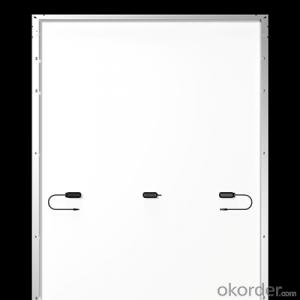
Product Show


Package
Typical package for one carton contains 1,200 cells. The cells are sealed in cell box every 100 pcs.
Gross weight per unit carton shall be around 16.4kg.
- Q:What is the role of surface coatings on solar silicon wafers?
- The role of surface coatings on solar silicon wafers is to enhance their performance and durability in solar cell applications. These coatings serve multiple purposes such as reducing surface reflectivity, improving light absorption, preventing surface contamination, increasing electrical conductivity, and protecting against environmental factors like humidity and corrosion. By enhancing the surface properties of silicon wafers, these coatings contribute to the overall efficiency and longevity of solar cells.
- Q:How are solar silicon wafers affected by surface passivation techniques?
- Surface passivation techniques have a significant impact on solar silicon wafers. These techniques aim to reduce the recombination of charge carriers at the surface of the wafers, thereby increasing their efficiency in converting sunlight into electricity. Passivation helps to minimize surface defects and traps, ensuring better electron-hole separation and reducing the loss of electrical energy. Overall, surface passivation techniques play a crucial role in enhancing the performance and overall effectiveness of solar silicon wafers.
- Q:Why the resistivity of silicon wafer is high and low
- If the thermistor is more normal. For example, when you hold your hands
- Q:What is the purpose of a busbar in a solar silicon wafer?
- The purpose of a busbar in a solar silicon wafer is to collect and distribute the electrical current generated by the photovoltaic cells. It acts as a conductor that connects the individual cells within the wafer, allowing the flow of electricity to be efficiently gathered and directed towards the desired output.
- Q:For solar wafer cutting diamond wire, what are the characteristics?
- There are several kinds of electroplated diamond wire, resin bonded diamond wire and mechanical pressing diamond wire. The general application of electroplating diamond wire is mainly due to its good wear resistance and heat resistance, diamond particles are not easy to fall off.Advantages: 1. Compared with the free abrasive cutting, the diamond wire cutting has a higher grinding speed, that is, higher production efficiency.2, silicon wafer yield is higher.3, cutting fluid consumption less, can reduce environmental pollution problems.Disadvantages: 1, the silicon wafer surface has obvious line, to see whether the customer can accept.
- Q:How do solar silicon wafers contribute to the overall efficiency of a solar panel?
- Solar silicon wafers play a crucial role in enhancing the overall efficiency of a solar panel. These wafers, made from highly purified silicon, absorb sunlight and convert it into electricity through the photovoltaic effect. The quality and characteristics of the silicon wafers directly impact the panel's ability to efficiently capture and convert solar energy. By maximizing light absorption and minimizing energy losses, high-quality silicon wafers significantly contribute to improving the overall efficiency and performance of a solar panel.
- Q:Process flow of wafer wafer ultrasonic cleaning machine?
- Plasma cleaning relates to the field of etching technology, and fully satisfies the removal of residual surface of silicon wafer after etching processKeep particle cleaningBackground technologyIn the etching process, the particles come from many sources: etching gas such as Cl2, HBr, CF4 etc. are corrosive, etching after the end will have a certain number of particles on the surface of the silicon wafer reaction chamber; a quartz cover will produce quartz particles in plasma bombardment; reaction chamber liner (liner) also metal particles will be produced in the etching process for long time. The surface residual silicon etching after particles block conductive connection, cause damage to the device. Therefore, the control of particles is very important in the etching process.
- Q:What is the role of solar silicon wafers in reducing reliance on fossil fuels?
- Solar silicon wafers play a crucial role in reducing reliance on fossil fuels by serving as the key component in the production of solar cells. These wafers are made from highly purified silicon, which, when exposed to sunlight, generates electricity through the photovoltaic effect. By harnessing solar energy, these wafers enable the generation of clean and renewable electricity, reducing the need for fossil fuel-based power generation. This helps in mitigating greenhouse gas emissions and combating climate change, thus reducing our overall dependence on fossil fuels for energy production.
- Q:How do solar silicon wafers handle shading or partial obstruction?
- Solar silicon wafers are generally designed to handle shading or partial obstruction fairly well. However, shading or obstruction can significantly reduce the overall efficiency and power output of solar panels. When a silicon wafer is shaded or partially obstructed, the affected cells produce less electricity, resulting in a decrease in the panel's performance. In some cases, shading can cause hotspots on the cells, leading to potential damage or reduced lifespan of the panel. To minimize the impact of shading, solar panels often incorporate bypass diodes, which redirect the current flow around the shaded cells, allowing the unshaded cells to generate electricity efficiently. Additionally, proper placement and orientation of solar panels can help minimize shading from nearby objects, maximizing their overall performance.
- Q:How do solar silicon wafers compare to other types of solar cells?
- Solar silicon wafers are the most commonly used material for manufacturing solar cells due to their high efficiency and reliability. Compared to other types of solar cells, such as thin-film or organic cells, silicon wafers have a higher conversion efficiency, meaning they can generate more electricity from sunlight. Additionally, silicon wafers have a longer lifespan and better durability, making them a preferred choice for long-term solar energy production.
1. Manufacturer Overview |
|
|---|---|
| Location | |
| Year Established | |
| Annual Output Value | |
| Main Markets | |
| Company Certifications | |
2. Manufacturer Certificates |
|
|---|---|
| a) Certification Name | |
| Range | |
| Reference | |
| Validity Period | |
3. Manufacturer Capability |
|
|---|---|
| a)Trade Capacity | |
| Nearest Port | |
| Export Percentage | |
| No.of Employees in Trade Department | |
| Language Spoken: | |
| b)Factory Information | |
| Factory Size: | |
| No. of Production Lines | |
| Contract Manufacturing | |
| Product Price Range | |
Send your message to us
156*156mm 3BB Mono-crystalline Silicon Solar Cell
- Ref Price:
-
- Loading Port:
- China main port
- Payment Terms:
- TT OR LC
- Min Order Qty:
- 100 watt
- Supply Capability:
- 10000 watt/month
OKorder Service Pledge
OKorder Financial Service
Similar products


New products
Hot products


Hot Searches
Related keywords

