
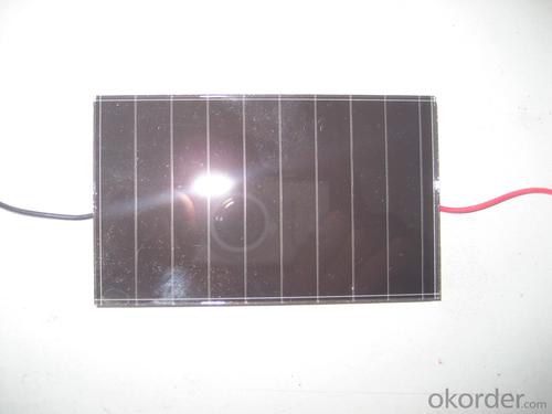
Amorphous silicon dice specification 5
- Ref Price:
-

- Loading Port:
- China Main Port
- Payment Terms:
- TT OR LC
- Min Order Qty:
- -
- Supply Capability:
- -
OKorder Service Pledge
OKorder Financial Service
You Might Also Like


Pv modules at present, the mainstream products are still in silicon as the main raw materials, only in terms of silicon raw material consumption, production 1 mw of crystalline silicon solar cell, need 10 to 12 tons of high purity silicon, but if use the same silicon materials used to produce thin film amorphous silicon solar cell can produce more than 200 mw.
From the perspective of energy consumption, amorphous silicon solar battery only 1-1.5 years of energy recovery period, more embodies its contribution to energy saving in the manufacturing process.
Component occupies a high proportion of costs in a photovoltaic system, the component prices directly affect the system cost, and thus affect the cost of photovoltaic power generation. Calculated at the current price of components, the same money, buy amorphous silicon products, you can get more close to 30% of the power components.
2, more power
For the same power of solar cell array, amorphous silicon solar cell is about 10% more than monocrystalline silicon, polycrystalline silicon battery power. This has been the Uni - Solar System LLC, Energy Photovoltaic Corp., Japan's Kaneka Corp., the Netherlands Energy research institute, and other organizations and experts confirmed that the Photovoltaic industry.
In sunny, that is to say, under the high temperature, amorphous silicon solar cell components can show more excellent power performance.
3, better low light response
Due to the characteristics of amorphous silicon atoms are arranged disorderly, the electron transition no longer comply with the restriction of traditional \"selection rule\", as a result, its light absorption characteristics and there are big differences monocrystalline silicon material. Amorphous silicon and monocrystalline silicon material absorption curve as shown
, amorphous silicon absorption curve has obvious three sections (A, B, C). Area A corresponding electronic transition between localized states, such as the gap state near Fermi level and to the tail state transition, the absorption coefficient is small, about 1-10 cm - 1, for this is absorbing; B area absorption coefficient with the increase of the photon energy index rose, it corresponds to the electrons from the valence band edge extension state to the conduction band localized state transition, as well as the localized electrons from the valence band tail states guide for edge extension state transition, the region's energy range is usually only about half of the electron volts, but absorption coefficient across two or three orders of magnitude, usually up to 104 cm - 1; Area C corresponds to the electrons from the valence band to the conduction band internal internal transition, the absorption coefficient is bigger, often in more than 104 cm - 1. After two absorption area is crystalline silicon eigen absorption area.
Can be seen in the figure, the intersection of two curves about 1.8 ev. It is important to note that in the visible light range (1.7 to 3.0 ev), the absorption coefficient of amorphous silicon material is almost an order of magnitude larger than the single crystal silicon. That is to say, in the morning the first part of the sun is not too strong, the second half, and it's cloudy in the afternoon under the condition of low light intensity, long wave is greater, the amorphous silicon material still has a large absorption coefficient. Again considering the amorphous silicon band gap is larger, the reverse saturation current I0 is smaller. And as mentioned the amorphous silicon battery the characteristics I - V characteristic curve of the amorphous silicon solar cell both in theory and in practical use in low light intensity has good adaptation.
• I - V characteristics of amorphous silicon cells after more than a Vm with the voltage drop slowly
In order to be convenient, we draw the I - V characteristics of two kinds of batteries on the same picture. Crystalline silicon and amorphous silicon battery I - V characteristics of general shape as shown
we see from the picture, two kinds of cells in the curve changes after exceed the maximum output power point gap is bigger. Output current of crystalline silicon cells after exceed the maximum output power point will soon fall to zero, curve steep; Rather than crystalline silicon cells output current after a long distance to fall to zero, the curve is relatively flat. Two kinds of battery Vm equivalent to about 83% of its open circuit voltage and 83% respectively.
when light intensity gradually become hour, short circuit current and open circuit voltage of solar battery will be stronger. Short circuit current decreases faster, of course, open circuit voltage decrease more slowly.
do in battery solar cell array under the condition of load, when the sun battery array of effective output voltage less than the terminal voltage of battery, battery cannot be recharged. When the light intensity gradually become hour, crystal silicon battery charging does not meet the conditions, and amorphous silicon due to the larger voltage difference, do not charge until the light is very dark, effectively increase the use of sunlight time. So, amorphous silicon cells to produce more electricity than the crystalline silicon.
4, more excellent high temperature performance
High in the outdoor environment temperature, amorphous silicon solar cell performance change, depends on the temperature, spectrum, as well as other related factors. But what is certain is: amorphous silicon than monocrystalline silicon or polycrystalline silicon are less likely to be affected by temperature.
Amorphous silicon solar cells than monocrystalline silicon, polycrystalline silicon cells have relatively small temperature coefficient of amorphous silicon solar cell output power best Pm temperature coefficient is about 0.19%, and monocrystalline silicon, polycrystalline silicon cells best output power Pm temperature coefficient is about 0.5%, when the battery work at higher temperatures, the two batteries will be a drop in the Pm, but the decline is different. They can be calculated using the following formula.
- Q:Can solar silicon wafers be used in solar-powered electric vehicles?
- Yes, solar silicon wafers can be used in solar-powered electric vehicles. These wafers are commonly used in the production of solar panels, which can be installed on the roof or exterior of electric vehicles to harness solar energy and supplement the vehicle's battery power. This allows for increased energy efficiency and reduced reliance on traditional charging methods for electric vehicles.
- Q:What specific steps should be used to clean the wafer? A little more detail
- LED (Light Emitting Diode), light emitting diode, referred to as LED, is a kind of power can be converted into visible light solid-state semiconductor devices, which can directly convert electricity into light. The heart of LED is a semiconductor chip, one end of which is attached to a support, one end is a negative electrode, and the other end is connected with the positive electrode of the power supply so that the whole chip is encapsulated by epoxy resin. The semiconductor chip is made up of two parts, one part is the P type semiconductor, in which the hole is dominant, the other end is the N type semiconductor.
- Q:What is the role of gettering in solar silicon wafers?
- The role of gettering in solar silicon wafers is to reduce or eliminate impurities and defects that can hinder the performance and efficiency of solar cells. Gettering helps to trap and remove unwanted impurities and contaminants, such as metal impurities and dislocations, from the bulk silicon material. This process ensures that the silicon wafers used in solar cells have a higher purity level, leading to improved electrical conductivity and overall performance of the solar cells.
- Q:Can solar silicon wafers be customized for specific solar panel designs?
- Yes, solar silicon wafers can be customized for specific solar panel designs. The size, shape, thickness, and other properties of the silicon wafers can be tailored to meet the requirements of different solar panel designs, allowing for optimized performance and integration.
- Q:How is a power optimizer integrated into a solar silicon wafer?
- A power optimizer is typically integrated into a solar silicon wafer by connecting it between the individual solar cells and the junction box. The power optimizer acts as a DC-DC converter, optimizing the power output of each individual solar cell by constantly tracking and adjusting the maximum power point. This optimization process allows for increased energy production and better performance, even in cases where the solar panels are not perfectly aligned or shaded.
- Q:What is the role of a solar silicon wafer in a solar cell?
- The role of a solar silicon wafer in a solar cell is to serve as the substrate or base material on which the photovoltaic (PV) cells are built. The wafer acts as a platform for the formation of the solar cell's semiconductor layers, which are responsible for converting sunlight into electricity. The silicon material used in the wafer possesses unique properties that make it an ideal choice for solar cells, such as its ability to efficiently absorb and convert solar energy. Ultimately, the solar silicon wafer plays a crucial role in enabling the production of renewable and sustainable energy through solar cells.
- Q:What is the role of a power optimizer in a solar silicon wafer?
- The role of a power optimizer in a solar silicon wafer is to enhance the overall performance and efficiency of the solar panel system. It optimizes the power output by ensuring that each individual solar module operates at its maximum power point, mitigating shading or mismatch issues, and reducing any losses caused by partial shading or dirt buildup. This technology helps to maximize the energy production, improve system reliability, and increase the overall return on investment for the solar installation.
- Q:4 inch polished silicon wafer thickness of 250um, after polishing the thickness of 6 inches of 300um, the current use of wax free polishing process often fragments, to find a solution!
- You can use the U.S. ZeroMicron wax free polishing template to solve the problem of non wax polishing fragments
- Q:How do solar silicon wafers contribute to reducing the reliance on imported energy?
- Solar silicon wafers contribute to reducing the reliance on imported energy by enabling the production of solar panels, which generate electricity from sunlight. By harnessing the power of the sun, solar panels reduce the need for electricity generated from fossil fuels, thus decreasing the dependence on imported energy sources. Additionally, as silicon wafers are a key component in solar panel manufacturing, their production and usage promote the growth of the domestic solar industry, further reducing reliance on imported energy.
- Q:How are solar silicon wafers connected to form a solar panel?
- Solar silicon wafers are connected to form a solar panel through a process called soldering. Thin metal strips, typically made of silver or aluminum, are soldered onto the front and back surfaces of the wafers. These metal strips, known as busbars, act as electrical conductors, connecting the wafers in series or parallel. This series or parallel configuration allows for the desired voltage and current output of the solar panel. Once the wafers are connected, they are then encapsulated in a protective layer and mounted onto a frame to create a complete solar panel.
1. Manufacturer Overview |
|
|---|---|
| Location | |
| Year Established | |
| Annual Output Value | |
| Main Markets | |
| Company Certifications | |
2. Manufacturer Certificates |
|
|---|---|
| a) Certification Name | |
| Range | |
| Reference | |
| Validity Period | |
3. Manufacturer Capability |
|
|---|---|
| a)Trade Capacity | |
| Nearest Port | |
| Export Percentage | |
| No.of Employees in Trade Department | |
| Language Spoken: | |
| b)Factory Information | |
| Factory Size: | |
| No. of Production Lines | |
| Contract Manufacturing | |
| Product Price Range | |
Send your message to us
Amorphous silicon dice specification 5
- Ref Price:
-
- Loading Port:
- China Main Port
- Payment Terms:
- TT OR LC
- Min Order Qty:
- -
- Supply Capability:
- -
OKorder Service Pledge
OKorder Financial Service
Similar products


New products
Hot products


Hot Searches
Related keywords

