
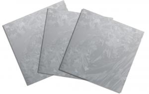
Polycrystalline/ Multiple Solar Silicon Wafer156*156, Solar Wafers
- Ref Price:
-

- Loading Port:
- Shanghai Port
- Payment Terms:
- TT or LC
- Min Order Qty:
- 100 Pieces PCS
- Supply Capability:
- 700MW/Per Year PCS/month
OKorder Service Pledge
Quality Product, Order Online Tracking, Timely Delivery
OKorder Financial Service
Credit Rating, Credit Services, Credit Purchasing
You Might Also Like


Specifications of Polycrystalline Silicon Wafer
Format : 156 mm × 156 mm ± 0.5 mm
Thickness : 200μm ± 10 μm
| Product name | Poly Wafer |
| Conductive type | P Type |
| Square size wafer (mm) | 156×156±0.5 |
| 219.20±0.5 | |
| Corner (mm)
|
1±0.5、45°±10º |
| 200±20 | |
| Total thickness(um) | ≤40 |
| Resistivity ranges(Ωcm) | 1-3 |
| Doping elements | boron |
| Carbon content(atoms/cc) | ≤8*1017 |
| Oxygen content(atoms/cc) | ≤1*1018 |
| Lifetime(μs) | ≥2 |
| Surface quality | No crack, gap, missing Angle, perforated, window, microcrystalline |
| Warping degrees(μm) | ≤50 |
| Neighbouring vertical degree | 90±0.5° |
| Side damage(mm) | ≤0.5mm(length)×0.3mm(width),(not more than 2 per wafer) |
| Line mark(μm) | ≤15 |
Usage and Applications of Poly Wafers
Poly Solar Wafers mainly used in Poly Solar Cells, with high efficiency and reliable quality. Our Wafer can promise the 25 years life span and have passed PID test.
Packaging & Delivery of Poly Wafers
Carton Box Package and Deliver by air
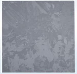
Factory Picture of Poly Wafers

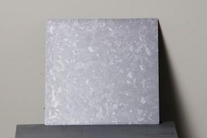
Package Picture of Poly Wafers

- Q:What is the purpose of an anti-reflective coating on a solar silicon wafer?
- The purpose of an anti-reflective coating on a solar silicon wafer is to minimize the amount of light reflection and maximize the amount of light absorption by the wafer. This coating helps to increase the overall efficiency of the solar cell by allowing more sunlight to pass through and be converted into electricity.
- Q:What is the production capacity of solar silicon wafers worldwide?
- The production capacity of solar silicon wafers worldwide is estimated to be in the range of tens of gigawatts (GW) per year.
- Q:How much a piece of silicon on the board
- The same power, the conversion rate of the area is small, or vice versa. If you do not consider the area, the same power, the amount of electricity generated is the same, with the high conversion rate and the low rate of change, of course, there will be some impact on life expectancy. I do not know so clear? I is a professional manufacturer of solar photovoltaic, do not understand what I can find, you can.
- Q:What is the role of gettering in solar silicon wafers?
- The role of gettering in solar silicon wafers is to remove impurities and defects from the material, thereby improving the efficiency and performance of the solar cells. Gettering helps to capture and immobilize impurities, such as metal impurities or oxygen, that can adversely affect the electrical properties of the silicon. By creating gettering sites, these impurities are attracted and trapped, allowing for the production of high-quality silicon wafers with enhanced solar cell performance.
- Q:What is the current industry standard for solar silicon wafer thickness?
- The current industry standard for solar silicon wafer thickness ranges from 180 to 200 micrometers.
- Q:Why integrated circuits are rectangular and the silicon chips are round
- The disk that you see is a wafer. This disk is not only the production of a chip, but N multiple chips are produced in this disk.
- Q:How are solar silicon wafers protected from fire or overheating?
- Solar silicon wafers are protected from fire or overheating through various measures, including the use of fire-resistant encapsulation materials and thermal management systems. These encapsulation materials, such as EVA (ethylene-vinyl acetate) or PVB (polyvinyl butyral), act as a protective layer around the solar cells, preventing direct contact with air and reducing the risk of fire. Additionally, thermal management systems, such as heat sinks or cooling fans, are employed to dissipate excess heat generated during operation, ensuring the wafers remain within a safe temperature range and minimizing the chances of overheating.
- Q:What is the expected degradation rate of solar silicon wafers over time?
- The expected degradation rate of solar silicon wafers over time varies depending on various factors such as the quality of the silicon material, manufacturing process, environmental conditions, and maintenance practices. However, on average, silicon solar wafers experience a degradation rate of around 0.5-1% per year. This means that after 25 to 30 years, solar panels may have lost around 20-30% of their original efficiency. It's important to note that advancements in technology and improved manufacturing processes are continuously reducing degradation rates, ultimately increasing the lifespan and efficiency of solar panels.
- Q:What is the expected efficiency improvement for perovskite solar silicon wafers?
- The expected efficiency improvement for perovskite solar silicon wafers is significant, with potential gains of up to 25-30% compared to traditional silicon-based solar cells.
- Q:How do solar silicon wafers compare to other types of solar cell technologies?
- Solar silicon wafers are the most widely used and dominant technology in the solar cell industry. They offer high efficiency and reliability, providing stable power output over a long lifespan. While other types of solar cell technologies, such as thin-film and organic cells, may have certain advantages like flexibility and lower production costs, they generally have lower efficiency and shorter lifespans compared to silicon wafers. Thus, in terms of overall performance and market adoption, solar silicon wafers remain the preferred choice for solar cell technology.
Our company is a world class resources and green energy developer, operator and supplier with its engagement in green energy development, integration and operation. We strives to offer highly efficient, eco-friendly, economical and reliable energy solutions through an integrated and diversified energy industrial chain. In adherence to the philosophy of bringing green power to life, the Group stays committed to continuously providing high-quality energy and services for a better living environment. Under approaches of people-oriented, excellence-foremost, value-creation and harmony-pursuant, our Group is determined to become a respected world-class green energy conglomerate.
1. Manufacturer Overview |
|
|---|---|
| Location | |
| Year Established | |
| Annual Output Value | |
| Main Markets | |
| Company Certifications | |
2. Manufacturer Certificates |
|
|---|---|
| a) Certification Name | |
| Range | |
| Reference | |
| Validity Period | |
3. Manufacturer Capability |
|
|---|---|
| a)Trade Capacity | |
| Nearest Port | |
| Export Percentage | |
| No.of Employees in Trade Department | |
| Language Spoken: | |
| b)Factory Information | |
| Factory Size: | |
| No. of Production Lines | |
| Contract Manufacturing | |
| Product Price Range | |
Send your message to us
Polycrystalline/ Multiple Solar Silicon Wafer156*156, Solar Wafers
- Ref Price:
-
- Loading Port:
- Shanghai Port
- Payment Terms:
- TT or LC
- Min Order Qty:
- 100 Pieces PCS
- Supply Capability:
- 700MW/Per Year PCS/month
OKorder Service Pledge
Quality Product, Order Online Tracking, Timely Delivery
OKorder Financial Service
Credit Rating, Credit Services, Credit Purchasing
Similar products


New products
Hot products


Hot Searches

