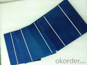
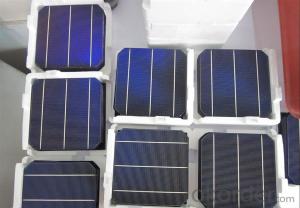
High Current Solar Cell 17.2% Polycrystalline Silicon Solar Cell Price
- Ref Price:
-

- Loading Port:
- Shanghai
- Payment Terms:
- TT OR LC
- Min Order Qty:
- 1000 pc
- Supply Capability:
- 100000 pc/month
OKorder Service Pledge
OKorder Financial Service
You Might Also Like


4 Bus Bars 156*156 17.6% efficiency poly solar cell
PHYSICAL CHARACTERISTICS
Dimension: 156mm x 156mm ± 0.5mm
Wafer Thickeness: 180um+20um and 200um+20um
Front(-) Four 1.2mm silver busbar
Silicon nitride blue anti-reflection coating
Back(+) aluminum back surface field
1.75mm(silver) wide segment soldering pads

Typical Electrical Characteristics
Efficiency | W(Pmpp) | V(Umpp) | A(Impp) | V(Uoc) | A(Isc) |
17.4-17.5 | 4.234 | 0.517 | 8.231 | 0.622 | 8.759 |
17.5-17.6 | 4.259 | 0.519 | 8.243 | 0.623 | 8.769 |
17.7-17.8 | 4.283 | 0.521 | 8.256 | 0.625 | 8.779 |
17.8-17.9 | 4.307 | 0.523 | 8.268 | 0.626 | 8.788 |
17.9-18.0 | 4.332 | 0.525 | 8.281 | 0.627 | 8.798 |
18.0-18.1 | 4.380 | 0.529 | 8.306 | 0.629 | 8.808 |
18.1-18.2 | 4.405 | 0.531 | 8.318 | 0.632 | 8.818 |
18.2-18.3 | 4.429 | 0.533 | 8.331 | 0.633 | 8.837 |
18.3-18.4 | 4.453 | 0.535 | 8.344 | 0.634 | 8.847 |
18.4-18.5 | 4.478 | 0.537 | 8.356 | 0.636 | 8.856 |
18.5-18.6 | 4.502 | 0.539 | 8.369 | 0.637 | 8.866 |
Efficiency | W(Pmpp) | V(Umpp) | A(Impp) | V(Uoc) | A(Isc) |
20.90-21.00 | 5.06 | 0.557 | 9.007 | 0.653 | 9.688 |
20.80-20.90 | 5.04 | 0.556 | 9.062 | 0.652 | 9.683 |
20.70-20.80 | 5.02 | 0.554 | 9.055 | 0.651 | 9.684 |
20.60-20.70 | 4.99 | 0.552 | 9.033 | 0.651 | 9.672 |
20.50-20.60 | 4.97 | 0.550 | 9.002 | 0.650 | 9.673 |
20.40-20.50 | 4.94 | 0.548 | 9.012 | 0.649 | 9.674 |
20.30-20.40 | 4.92 | 0.546 | 9.009 | 0.649 | 9.655 |
20.20-20.30 | 4.89 | 0.543 | 9.012 | 0.648 | 9.634 |
20.10-20.20 | 4.87 | 0.541 | 8.998 | 0.648 | 9.617 |
20.00-20.10 | 4.85 | 0.540 | 8.977 | 0.647 | 9.600 |
*Data under standard testing conditional (STC):1,000w/m2,AM1.5, 25°C , Pmax:Positive power tolerance.
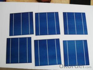
3 Bus Bars 156*156 17.4% efficiency poly solar cell
Dimension: 156 mm x 156 mm ± 0.5 mm
Wafer Thickeness: 156 mm x 156 mm ± 0.5 mm

Typical Electrical Characteristics:
| Efficiency code | 1660 | 1680 | 1700 | 1720 | 1740 | 1760 | 1780 | 1800 | 1820 | 1840 | 1860 |
| Efficiency (%) | 16.6 | 16.8 | 17.0 | 17.2 | 17.4 | 17.6 | 17.8 | 18.0 | 18.2 | 18.4 | 18.6 |
| Pmax (W) | 4.04 | 4.09 | 4.14 | 4.19 | 4.23 | 4.28 | 4.33 | 4.38 | 4.43 | 4.48 | 4.53 |
| Voc (V) | 0.612 | 0.615 | 0.618 | 0.621 | 0.624 | 0.627 | 0.629 | 0.63 | 0.633 | 0.635 | 0.637 |
| Isc (A) | 8.42 | 8.46 | 8.51 | 8.56 | 8.61 | 8.65 | 8.69 | 8.73 | 8.77 | 8.81 | 8.84 |
| Imp (A) | 7.91 | 7.99 | 8.08 | 8.16 | 8.22 | 8.27 | 8.33 | 8.38 | 8.43 | 8.48 | 8.53 |
* Testing conditions: 1000 W/m2, AM 1.5, 25 °C, Tolerance: Efficiency ± 0.2% abs., Pmpp ±1.5% rel.
* Imin : at 0.5 V
Production:

Package:

FAQ:
1. Q: Do you have your own factory?
A: Yes, we have. Our factory located in Jiangsu
2. Q: How can I visit your factory?
A: Before you visit,please contact us.We will show you the route or arrange a car to pick you up.
3. Q: Do you provide free sample?
A: Commenly we provide paid sample.
4. Q: Could you print our company LOGO on the nameplate and package?
A: Yes, we accept it.And need an Authorization Letter from you.
5. Q: Do you accept custom design on size?
A: Yes, if the size is reasonable.
6. Q: How can I be your agent in my country?
A: Please leave feedback. It's better for us to talk about details by email.
7. Q: Do you have solar project engineer who can guide me to install system?
A: Yes, we have a professional engineer team. They can teach you how to install a solar system.
- Q:What is the role of solar silicon wafers in reducing the digital divide?
- Solar silicon wafers play a crucial role in reducing the digital divide by facilitating the production of affordable and sustainable solar panels. These panels can be used to generate electricity in remote and underserved areas where access to the power grid is limited. By harnessing solar energy, these communities can power devices such as computers, smartphones, and other digital technologies, thus bridging the gap in access to information and communication. Solar silicon wafers enable the production of cost-effective solar panels, expanding the reach of clean and renewable energy solutions, and contributing to narrowing the digital divide.
- Q:Can solar silicon wafers be used in military or defense applications?
- Yes, solar silicon wafers can be used in military or defense applications. They can be integrated into various military equipment and systems such as remote sensors, surveillance systems, unmanned aerial vehicles (UAVs), and portable power systems for soldiers in the field. Solar silicon wafers provide a reliable and sustainable source of power in remote or hostile environments, reducing the dependence on traditional fuel sources and increasing operational capabilities.
- Q:How do solar silicon wafers contribute to reducing carbon emissions?
- Solar silicon wafers contribute to reducing carbon emissions by enabling the production of solar panels, which generate clean and renewable energy from sunlight. As the key component of solar cells, silicon wafers capture sunlight and convert it into electricity without emitting any greenhouse gases or pollutants. This technology reduces the dependence on fossil fuels, such as coal or gas, which emit carbon dioxide when burned for energy production. By harnessing solar power through silicon wafers, we can decrease the overall carbon footprint and mitigate climate change.
- Q:What are the different types of anti-reflective coatings used on solar silicon wafers?
- There are primarily two types of anti-reflective coatings used on solar silicon wafers: silicon nitride (SiN) and titanium dioxide (TiO2) coatings. These coatings help reduce the reflection of sunlight, thereby increasing the efficiency of solar cells by allowing more light to be absorbed.
- Q:Can solar silicon wafers be used in other electronic devices?
- Yes, solar silicon wafers can be used in other electronic devices. While they are primarily used in solar panels to convert sunlight into electricity, they can also be used in various other electronic applications such as sensors, integrated circuits, and batteries. The properties of solar silicon wafers, such as their high purity and efficient light absorption, make them suitable for a wide range of electronic devices beyond just solar panels.
- Q:How to calculate the conversion efficiency of monocrystalline silicon
- Proportion of dark current - Irev>6 cell ratioThe proportion of low efficiency tablets - the proportion of P156Eff<14.5% batteries8 inch single crystal conversion rate of about 18.5%; a single conversion rate of about 9 inches in about 18.6%; quasi single crystal (large particles) probably about 18%; the new diamond wire cutting rate can be converted to about 18.92%.
- Q:Can solar silicon wafers be used in harsh environments?
- Yes, solar silicon wafers can be used in harsh environments. They are designed to withstand various environmental conditions such as extreme temperatures, high humidity, and exposure to UV radiation. The wafers are typically coated with protective materials to enhance their durability and resistance to corrosion, making them suitable for harsh outdoor environments.
- Q:What is the effect of fill factor on the efficiency of a solar silicon wafer?
- The fill factor is an important parameter that affects the efficiency of a solar silicon wafer. It represents the degree to which the solar cell can convert incident light into electrical energy. A higher fill factor generally leads to higher efficiency as it indicates less internal resistance and better utilization of the available sunlight. Therefore, a higher fill factor can result in improved power output and overall performance of the solar silicon wafer.
- Q:What is the role of back surface field (BSF) on solar silicon wafers?
- The role of the back surface field (BSF) on solar silicon wafers is to reduce the recombination of charge carriers (electrons and holes) that occurs at the back surface of the wafer. By creating a high-doped region at the back surface, the BSF helps to enhance the efficiency of the solar cell by preventing the loss of generated charge carriers, thus improving the overall conversion of sunlight into electricity.
- Q:How are solar silicon wafers cleaned before assembly into solar cells?
- Solar silicon wafers are typically cleaned before assembly into solar cells using a multi-step cleaning process. This process involves several stages, such as chemical etching, rinsing, and drying. Initially, the wafers are immersed in a cleaning solution that removes any impurities or contaminants on their surfaces. Subsequently, they undergo rinsing with deionized water to eliminate any remaining residue. Finally, the wafers are carefully dried to ensure a clean and pristine surface before they are assembled into solar cells.
1. Manufacturer Overview |
|
|---|---|
| Location | |
| Year Established | |
| Annual Output Value | |
| Main Markets | |
| Company Certifications | |
2. Manufacturer Certificates |
|
|---|---|
| a) Certification Name | |
| Range | |
| Reference | |
| Validity Period | |
3. Manufacturer Capability |
|
|---|---|
| a)Trade Capacity | |
| Nearest Port | |
| Export Percentage | |
| No.of Employees in Trade Department | |
| Language Spoken: | |
| b)Factory Information | |
| Factory Size: | |
| No. of Production Lines | |
| Contract Manufacturing | |
| Product Price Range | |
Send your message to us
High Current Solar Cell 17.2% Polycrystalline Silicon Solar Cell Price
- Ref Price:
-
- Loading Port:
- Shanghai
- Payment Terms:
- TT OR LC
- Min Order Qty:
- 1000 pc
- Supply Capability:
- 100000 pc/month
OKorder Service Pledge
OKorder Financial Service
Similar products


New products
Hot products


Hot Searches
Related keywords

