


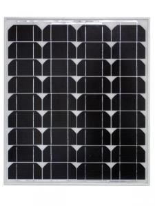
Solar Cell High Quality A Grade Cell Poly/Monocrystalline 5v
- Ref Price:
-

- Loading Port:
- Shanghai
- Payment Terms:
- TT OR LC
- Min Order Qty:
- 1000 pc
- Supply Capability:
- 100000 pc/month
OKorder Service Pledge
OKorder Financial Service
You Might Also Like


Specifications
hot sale solar cell
1.16.8%~18.25% high efficiency
2.100% checked quality
3.ISO9001/ISO14001/TUV/CE/UL
4.stable performance
We can offer you the best quality products and services, don't miss !
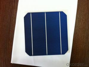
POLY6'(156*156)
Polycrystalline Silicon Solar cell
Physical Characteristics
Dimension: 156mm×156mm±0.5mm
Diagonal: 220mm±0.5mm
Thickness(Si): 200±20 μm
Front(-) Back(+)
Blue anti-reflecting coating (silicon nitride); Aluminum back surface field;
1.5mm wide bus bars; 2.0mm wide soldering pads;
Distance between bus bars: 51mm . Distance between bus bars :51mm .
Electrical Characteristics
Efficiency(%) | 18.00 | 17.80 | 17.60 | 17.40 | 17.20 | 16.80 | 16.60 | 16.40 | 16.20 | 16.00 | 15.80 | 15.60 |
Pmpp(W) | 4.33 | 4.29 | 4.24 | 4.19 | 4.14 | 4.09 | 4.04 | 3.99 | 3.94 | 3.90 | 3.86 | 3.82 |
Umpp(V) | 0.530 | 0.527 | 0.524 | 0.521 | 0.518 | 0.516 | 0.514 | 0.511 | 0.509 | 0.506 | 0.503 | 0.501 |
Impp(A) | 8.159 | 8.126 | 8.081 | 8.035 | 7.990 | 7.938 | 7.876 | 7.813 | 7.754 | 7.698 | 7.642 | 7.586 |
Uoc(V) | 0.633 | 0.631 | 0.628 | 0.625 | 0.623 | 0.620 | 0.618 | 0.617 | 0.615 | 0.613 | 0.611 | 0.609 |
Isc(A) | 8.709 | 8.677 | 8.629 | 8.578 | 8.531 | 8.478 | 8.419 | 8.356 | 8.289 | 8.220 | 8.151 | 8.083 |

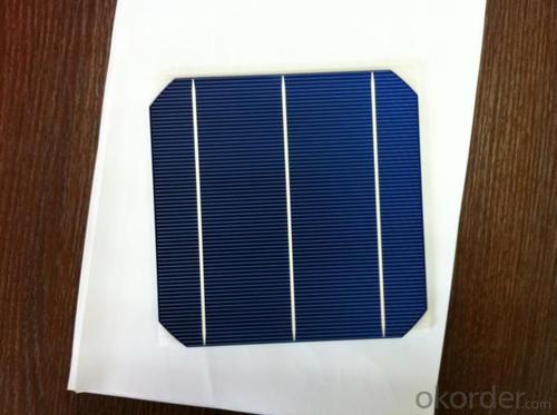
MONO5'(125*125mm)165
Monocrystalline silicon solar cell
Physical Characteristics
Dimension: 125mm×125mm±0.5mm
Diagonal: 165mm±0.5mm
Thickness(Si): 200±20 μm
Front(-) Back(+)
Blue anti-reflecting coating(silicon nitride); Aluminum back surface field;
1.6mmwide bus bars; 2.5mm wide soldering pads;
Distance between bus bars: 61mm . Distance between bus bars :61mm .
Electrical Characteristics
Efficiency(%) | 19.40 | 19.20 | 19.00 | 18.80 | 18.60 | 18.40 | 18.20 | 18.00 | 17.80 | 17.60 | 17.40 | 17.20 |
Pmpp(W) | 2.97 | 2.94 | 2.91 | 2.88 | 2.85 | 2.82 | 2.79 | 2.76 | 2.73 | 2.70 | 2.67 | 2.62 |
Umpp(V) | 0.537 | 0.535 | 0.533 | 0.531 | 0.527 | 0.524 | 0.521 | 0.518 | 0.516 | 0.515 | 0.513 | 0.509 |
Impp(A) | 5.531 | 5.495 | 5.460 | 5.424 | 5.408 | 5.382 | 5.355 | 5.328 | 5.291 | 5.243 | 5.195 | 4.147 |
Uoc(V) | 0.637 | 0.637 | 0.636 | 0.635 | 0.633 | 0.630 | 0.629 | 0.629 | 0.628 | 0.626 | 0.626 | 0.625 |
Isc(A) | 5.888 | 5.876 | 5.862 | 5.848 | 5.839 | 5.826 | 5.809 | 5.791 | 5.779 | 5.756 | 5.293 | 5.144 |

FAQ:
Q:How can i get some sample?
A:Yes , if you want order ,sample is not a problem.
Q:How about your solar panel efficency?
A: Our product efficency around 17.25%~18.25%.
Q:What’s the certificate you have got?
A: we have overall product certificate of ISO9001/ISO14001/CE/TUV/UL
- Q:What is the role of an interconnect in a solar silicon wafer?
- The role of an interconnect in a solar silicon wafer is to connect individual solar cells together in a series or parallel configuration, allowing for the efficient flow of electricity generated by the cells. It helps to establish electrical connections between the cells, ensuring that the current produced by each cell is combined and collected effectively.
- Q:Seeking for the video: manual insert silicon wafer single crystal insert method
- After the water is put into the plug, each time the number of slices can not be more than fifty pieces, the number of chips too easy to fall damaged silicon. If the chip is not cleaned in time to allow the silicon chip in the water bubble, but the bubble can not be more than an hour
- Q:Are solar silicon wafers recyclable?
- Yes, solar silicon wafers are recyclable.
- Q:There is a micro structure on the side of the silicon wafer
- For solar cells destined to enter the market market (mass) products, the advantages of reserves is also one of the main reasons for the silicon photovoltaic materials.
- Q:How are solar silicon wafers affected by light-induced annealing?
- Solar silicon wafers are positively affected by light-induced annealing. This process helps to reduce defects and improve the overall efficiency of the wafers by repairing crystal lattice damage caused during fabrication.
- Q:Can solar silicon wafers be used in solar-powered charging stations?
- Yes, solar silicon wafers can be used in solar-powered charging stations. These wafers are a key component in producing solar cells, which convert sunlight into electricity. Solar-powered charging stations utilize solar cells to capture sunlight and convert it into electrical energy to charge various devices. Therefore, solar silicon wafers play a crucial role in the functioning of solar-powered charging stations.
- Q:How are solar silicon wafers protected from bird droppings?
- Solar silicon wafers are typically protected from bird droppings through the installation of anti-reflective coatings on the surface, which make it difficult for bird droppings to adhere to the wafers. Additionally, regular cleaning and maintenance of solar panels can help prevent the accumulation of bird droppings, ensuring optimal performance and efficiency of the solar cells.
- Q:How is a solar silicon wafer made?
- A solar silicon wafer is made through a process called "solar-grade silicon purification" followed by "crystal growth" and "wafering". In the purification stage, impurities are removed from the raw silicon to obtain solar-grade silicon. Next, the purified silicon is melted and solidified to form a silicon crystal in the crystal growth stage. This crystal is then sliced into thin discs using a wire saw or diamond blade, resulting in the wafering stage. These wafers are then used as the base material for manufacturing solar cells.
- Q:How are solar silicon wafers protected from static electricity damage?
- Solar silicon wafers are protected from static electricity damage through the use of antistatic materials and precautions during handling and manufacturing processes. Antistatic coatings or films are applied to the wafers or their protective packaging to dissipate any static charges that may be present. Additionally, special packaging materials and procedures are utilized to minimize static electricity buildup and discharge during storage and transportation.
- Q:How are solar silicon wafers tested for resistivity and sheet resistance?
- Solar silicon wafers are tested for resistivity and sheet resistance using a variety of methods. One common technique is the four-point probe method, where four evenly spaced probes are placed on the surface of the wafer. A known current is passed between the outer probes, while the voltage is measured between the inner probes. By applying Ohm's law, the resistivity and sheet resistance can be calculated based on the measured current and voltage values. Another method involves using a Hall effect measurement, where a magnetic field is applied perpendicular to the wafer's surface and the resulting voltage is measured. This allows for the determination of the resistivity and sheet resistance. These testing methods help ensure the quality and performance of solar silicon wafers in photovoltaic applications.
1. Manufacturer Overview |
|
|---|---|
| Location | |
| Year Established | |
| Annual Output Value | |
| Main Markets | |
| Company Certifications | |
2. Manufacturer Certificates |
|
|---|---|
| a) Certification Name | |
| Range | |
| Reference | |
| Validity Period | |
3. Manufacturer Capability |
|
|---|---|
| a)Trade Capacity | |
| Nearest Port | |
| Export Percentage | |
| No.of Employees in Trade Department | |
| Language Spoken: | |
| b)Factory Information | |
| Factory Size: | |
| No. of Production Lines | |
| Contract Manufacturing | |
| Product Price Range | |
Send your message to us
Solar Cell High Quality A Grade Cell Poly/Monocrystalline 5v
- Ref Price:
-
- Loading Port:
- Shanghai
- Payment Terms:
- TT OR LC
- Min Order Qty:
- 1000 pc
- Supply Capability:
- 100000 pc/month
OKorder Service Pledge
OKorder Financial Service
Similar products


New products
Hot products


Hot Searches
Related keywords

