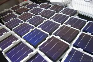


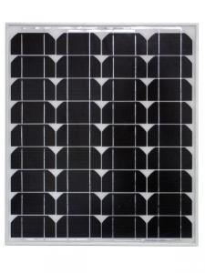
High Current Solar Cell 16.6% Polycrystalline Silicon Solar Cell Price
- Ref Price:
-

- Loading Port:
- Shanghai
- Payment Terms:
- TT OR LC
- Min Order Qty:
- 1000 pc
- Supply Capability:
- 100000 pc/month
OKorder Service Pledge
OKorder Financial Service
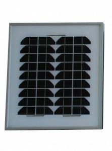
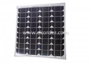
You Might Also Like


4 Bus Bars 156*156 17.6% efficiency poly solar cell
PHYSICAL CHARACTERISTICS
Dimension: 156mm x 156mm ± 0.5mm
Wafer Thickeness: 180um+20um and 200um+20um
Front(-) Four 1.2mm silver busbar
Silicon nitride blue anti-reflection coating
Back(+) aluminum back surface field
1.75mm(silver) wide segment soldering pads

Typical Electrical Characteristics
Efficiency | W(Pmpp) | V(Umpp) | A(Impp) | V(Uoc) | A(Isc) |
17.4-17.5 | 4.234 | 0.517 | 8.231 | 0.622 | 8.759 |
17.5-17.6 | 4.259 | 0.519 | 8.243 | 0.623 | 8.769 |
17.7-17.8 | 4.283 | 0.521 | 8.256 | 0.625 | 8.779 |
17.8-17.9 | 4.307 | 0.523 | 8.268 | 0.626 | 8.788 |
17.9-18.0 | 4.332 | 0.525 | 8.281 | 0.627 | 8.798 |
18.0-18.1 | 4.380 | 0.529 | 8.306 | 0.629 | 8.808 |
18.1-18.2 | 4.405 | 0.531 | 8.318 | 0.632 | 8.818 |
18.2-18.3 | 4.429 | 0.533 | 8.331 | 0.633 | 8.837 |
18.3-18.4 | 4.453 | 0.535 | 8.344 | 0.634 | 8.847 |
18.4-18.5 | 4.478 | 0.537 | 8.356 | 0.636 | 8.856 |
18.5-18.6 | 4.502 | 0.539 | 8.369 | 0.637 | 8.866 |
Efficiency | W(Pmpp) | V(Umpp) | A(Impp) | V(Uoc) | A(Isc) |
20.90-21.00 | 5.06 | 0.557 | 9.007 | 0.653 | 9.688 |
20.80-20.90 | 5.04 | 0.556 | 9.062 | 0.652 | 9.683 |
20.70-20.80 | 5.02 | 0.554 | 9.055 | 0.651 | 9.684 |
20.60-20.70 | 4.99 | 0.552 | 9.033 | 0.651 | 9.672 |
20.50-20.60 | 4.97 | 0.550 | 9.002 | 0.650 | 9.673 |
20.40-20.50 | 4.94 | 0.548 | 9.012 | 0.649 | 9.674 |
20.30-20.40 | 4.92 | 0.546 | 9.009 | 0.649 | 9.655 |
20.20-20.30 | 4.89 | 0.543 | 9.012 | 0.648 | 9.634 |
20.10-20.20 | 4.87 | 0.541 | 8.998 | 0.648 | 9.617 |
20.00-20.10 | 4.85 | 0.540 | 8.977 | 0.647 | 9.600 |
*Data under standard testing conditional (STC):1,000w/m2,AM1.5, 25°C , Pmax:Positive power tolerance.
3 Bus Bars 156*156 17.4% efficiency poly solar cell
Dimension: 156 mm x 156 mm ± 0.5 mm
Wafer Thickeness: 156 mm x 156 mm ± 0.5 mm

Typical Electrical Characteristics:
| Efficiency code | 1660 | 1680 | 1700 | 1720 | 1740 | 1760 | 1780 | 1800 | 1820 | 1840 | 1860 |
| Efficiency (%) | 16.6 | 16.8 | 17.0 | 17.2 | 17.4 | 17.6 | 17.8 | 18.0 | 18.2 | 18.4 | 18.6 |
| Pmax (W) | 4.04 | 4.09 | 4.14 | 4.19 | 4.23 | 4.28 | 4.33 | 4.38 | 4.43 | 4.48 | 4.53 |
| Voc (V) | 0.612 | 0.615 | 0.618 | 0.621 | 0.624 | 0.627 | 0.629 | 0.63 | 0.633 | 0.635 | 0.637 |
| Isc (A) | 8.42 | 8.46 | 8.51 | 8.56 | 8.61 | 8.65 | 8.69 | 8.73 | 8.77 | 8.81 | 8.84 |
| Imp (A) | 7.91 | 7.99 | 8.08 | 8.16 | 8.22 | 8.27 | 8.33 | 8.38 | 8.43 | 8.48 | 8.53 |
* Testing conditions: 1000 W/m2, AM 1.5, 25 °C, Tolerance: Efficiency ± 0.2% abs., Pmpp ±1.5% rel.
* Imin : at 0.5 V
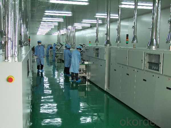
Production:

Package:

FAQ:
1. Q: Do you have your own factory?
A: Yes, we have. Our factory located in Jiangsu
2. Q: How can I visit your factory?
A: Before you visit,please contact us.We will show you the route or arrange a car to pick you up.
3. Q: Do you provide free sample?
A: Commenly we provide paid sample.
4. Q: Could you print our company LOGO on the nameplate and package?
A: Yes, we accept it.And need an Authorization Letter from you.
5. Q: Do you accept custom design on size?
A: Yes, if the size is reasonable.
6. Q: How can I be your agent in my country?
A: Please leave feedback. It's better for us to talk about details by email.
7. Q: Do you have solar project engineer who can guide me to install system?
A: Yes, we have a professional engineer team. They can teach you how to install a solar system.
- Q:What is the role of surface passivation layers on solar silicon wafers?
- The role of surface passivation layers on solar silicon wafers is to minimize the recombination of charge carriers, such as electrons and holes, at the surface of the wafer. These layers help improve the efficiency and performance of solar cells by reducing surface recombination losses, increasing the lifetime of charge carriers, and enhancing the overall electrical properties of the device.
- Q:How are solar silicon wafers protected from moisture during storage?
- Solar silicon wafers are typically protected from moisture during storage by being sealed in airtight containers or packaging materials that have low moisture permeability. This prevents any moisture from coming in contact with the wafers, which could potentially degrade their performance or cause damage. Additionally, desiccant packets or moisture-absorbing materials are commonly used inside the packaging to further minimize moisture levels and maintain the integrity of the wafers.
- Q:How do solar silicon wafers contribute to reducing the risk of power outages?
- Solar silicon wafers, which are the key component in solar panels, contribute to reducing the risk of power outages by harnessing solar energy and converting it into electricity. This renewable energy source helps diversify the power generation mix, reducing reliance on fossil fuels and decreasing the strain on the power grid. As solar panels generate electricity during the daytime, when demand is typically high, they help meet peak load requirements and prevent overloading or blackouts. By providing a decentralized and distributed energy source, solar silicon wafers enhance the resilience and reliability of the power system, mitigating the risk of power outages.
- Q:What is the role of solar silicon wafers in rural electrification?
- Solar silicon wafers play a crucial role in rural electrification by serving as the key component in solar photovoltaic panels. These wafers are responsible for converting sunlight into electricity, enabling the generation of clean and sustainable energy in remote rural areas. By harnessing solar power through the use of silicon wafers, rural communities gain access to reliable electricity, reducing their dependence on traditional and often unreliable sources such as diesel generators or kerosene lamps. This contributes to improving living conditions, promoting economic development, and reducing carbon emissions, ultimately supporting the goal of achieving universal energy access in rural areas.
- Q:What is the impact of impurities in solar silicon wafers on performance?
- Impurities in solar silicon wafers can have a significant impact on the performance of solar cells. These impurities, such as metal contaminants or dopants, can introduce defects in the crystal structure of the silicon, affecting the efficiency of electron movement and trapping photons. This can lead to reduced power output, decreased conversion efficiency, and shorter lifespan of the solar cells. Therefore, it is crucial to minimize impurities during the manufacturing process to optimize the performance and overall quality of solar silicon wafers.
- Q:What is the purpose of a busbar in a solar silicon wafer?
- The purpose of a busbar in a solar silicon wafer is to collect and distribute the electrical current generated by the photovoltaic cells. It acts as a conductor that connects the individual cells within the wafer, allowing the flow of electricity to be efficiently gathered and directed towards the desired output.
- Q:How does the thickness of a front contact affect the efficiency of a solar silicon wafer?
- The thickness of a front contact on a solar silicon wafer directly affects the efficiency of the wafer. A thicker front contact can reduce the efficiency of a solar cell because it can increase the amount of light that is reflected off the surface of the wafer, preventing it from being absorbed and converted into electricity. On the other hand, a thinner front contact can improve efficiency by allowing more light to be absorbed and utilized by the solar cell. Therefore, finding the optimal thickness for the front contact is crucial in maximizing the efficiency of a solar silicon wafer.
- Q:What are some of the silicon wafer factory
- The following is a silicon production company series positions distribution table, you can refer to the 1 equipment management department manager deputy manager of electrical equipment equipment maintenance engineer mechanical equipment maintenance Engineer Association and insurance technician equipment management maintenance team leader electric operation monitor operation duty electrician maintenance electrician maintenance mechanic subtotal
- Q:Are solar silicon wafers affected by shading?
- Yes, solar silicon wafers are indeed affected by shading. Shading on solar silicon wafers can significantly reduce the efficiency and performance of solar panels. When a part of the panel is shaded, it creates a mismatch in the current flow, resulting in energy loss. Therefore, it is essential to avoid shading to maximize the effectiveness of solar panels.
- Q:I grew up in the silicon chip Ag particles, the size of about a few hundred nanometers, I would like to ask how I do before the TEM sample?
- Alcohol is usually placed inside, with ultrasonic cleaning instrument scattered about, the purpose is to make the particles do not reunite together.
1. Manufacturer Overview |
|
|---|---|
| Location | |
| Year Established | |
| Annual Output Value | |
| Main Markets | |
| Company Certifications | |
2. Manufacturer Certificates |
|
|---|---|
| a) Certification Name | |
| Range | |
| Reference | |
| Validity Period | |
3. Manufacturer Capability |
|
|---|---|
| a)Trade Capacity | |
| Nearest Port | |
| Export Percentage | |
| No.of Employees in Trade Department | |
| Language Spoken: | |
| b)Factory Information | |
| Factory Size: | |
| No. of Production Lines | |
| Contract Manufacturing | |
| Product Price Range | |
Send your message to us
High Current Solar Cell 16.6% Polycrystalline Silicon Solar Cell Price
- Ref Price:
-
- Loading Port:
- Shanghai
- Payment Terms:
- TT OR LC
- Min Order Qty:
- 1000 pc
- Supply Capability:
- 100000 pc/month
OKorder Service Pledge
OKorder Financial Service
Similar products


New products
Hot products


Hot Searches
Related keywords

