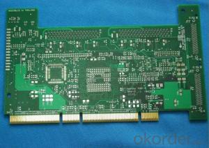


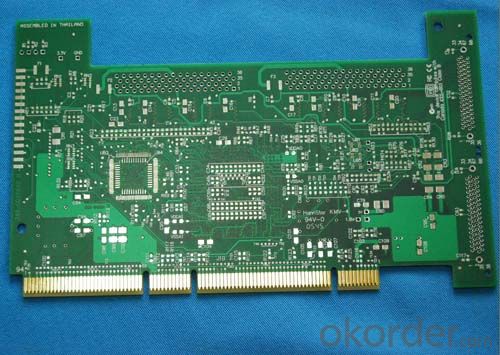
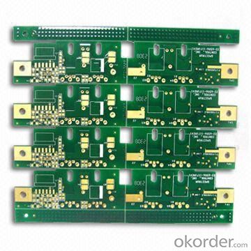

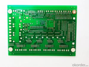
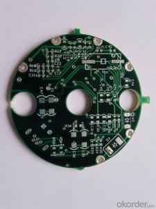
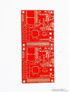
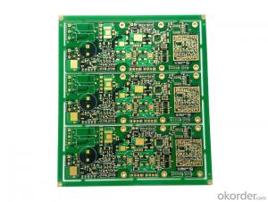
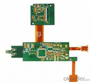
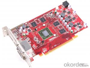
High quality 8 layer gold finger pcb, made in china
- Ref Price:
-

- Loading Port:
- Shanghai
- Payment Terms:
- TT OR LC
- Min Order Qty:
- 1 pc
- Supply Capability:
- 10000 pc/month
OKorder Service Pledge
OKorder Financial Service
You Might Also Like
Specification

Product Description
1. UL,ISO9001,ISO14001, TS16949 certificate
2. Short lead time.
3. PCB ROHS compliant.
4. Turkey service
Free Technology Support
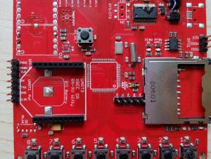
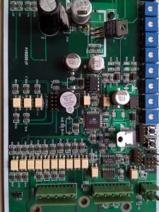
PCB Assembly
Turnkey service(PCB manufacture, components procurement and assembly)
Minimum lead time for assembly is only 5 days
Prototype building, No Minimum quantity Required
Reliable Parts
Surface mount, through hole, BGA, QFP, QFN …
ROHS compliant and lead-free process
PCB Capability
Material: FR4, CEM-3, Halogen Free, Rogers, High TG etc.
Layer counts: 1-18 layers
Finished Copper Thickness: 0.5-4 OZ
Finished Board Thickness: 0.2-5.0mm
Min. Line/Track Width: 4mil
Min. Line/Track Space: 4mil
Min. Contour Tolerance: +/-0.1mm
Min. Finished Diameter of PTH Hole: 0.2mm
Max. Board Thickness/Hole Ratio: 12:1
Min. Solder Mask Bridge: 4mil (Min. SMT Pad Space 8mil)
Min. Legend (Silk screen) Track Width: 5mil
Min. Legend (Silk screen) Height: 30mil
Min. drilling slot size: 0.6mm
Solder mask color: green, black, blue, white, yellow, purple, and matt, etc.
Legend/Silk screen Color: white, yellow, black, etc.
Surface Treatment: HAL, Lead Free HAL, Immersion gold, OSP, Immersion tin, Immersion silver, etc.
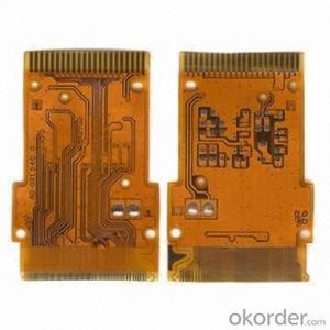
Other Technology: Gold finger, peelable mask, Non-across blind/buried vias, characteristic impedance control, Rigid-flex board etc.
Reliability Test: flying probe test/fixture test, impedance test, solderability test, thermal shock test, hole resistance test, and micro metallographic section analysis, etc.
Bow and twist: ≤1%
Flammability: 94V-0
4. Professional engineering staff to provide technical support.
5.OEM and ODM service are welcome.
Packaging Detail: Vacuum packaging
Delivery Time: 10-15 days
- Q: What is the light blue oil component used for brush circuit boards
- Generally through the membrane, graphics transfer, chemical etching, through-hole and copper processing, flux and solder processing technology.
- Q: Circuit board display device which
- Through Hole: There are metal vias and non-metallic vias, where metal vias are used to connect the components between the layers of the pins.
- Q: Protel pcb how to rotate the board?
- It includes circuit schematic drawing, analog circuit and digital circuit mixed signal simulation, multi-layer printed circuit board design, programmable logic device design, chart generation,
- Q: PCB board in the multi-layer is what it means
- Since the drilling and plating have been completed before all the layers have been rolled together, this technique has violated the traditional production process from the outset. The innermost two layers consist of a conventional double-sided panel, while the outer layers are different, and they are made of separate single-sided panels.
- Q: What are the materials used for the Merrillas on PCB circuit boards?
- Mylar sheet (MYLAR film) is a PET polyester film, it is by the dimethyl terephthalate and ethylene glycol in the relevant catalyst with the help of heating, after ester exchange and vacuum polycondensation, biaxial stretching film.
- Q: Protel how to lock all components
- running in the DOS environment, the hardware requirements are very low, no hard disk 286 1M memory can run, but its function is less, only the circuit schematic Drawing and PCB design function, the printed circuit board automatic distribution of the cloth rate is low, and today's PROTEL has been developed to DXP 2004, is a huge EDA software,
- Q: There are several main circuit board process
- Material production - open material --- inner line - press - mechanical drilling - plating - outer line - anti-welding - text --- surface treatment - molding --- test - Appearance inspection --- packaging shipping
- Q: What is the working principle of the circuit board?
- Circuit board works: the electronic components on the fixed and connected into the circuit. Circuit board name: circuit boards, PCB board, aluminum plate, high frequency board, thick copper plate, impedance board, PCB, ultra-thin circuit boards, ultra-thin circuit boards, printing (copper etching technology) circuit boards.
- Q: Double-sided circuit board, what is the hole ah
- The buried hole refers to the connection hole located in the inner layer of the printed circuit board and does not extend to the surface of the circuit board.
- Q: PCB circuit board has several materials?
- Its development has been 100 years of history; its design is mainly layout design; the main advantage of using the circuit board is to greatly reduce the wiring and assembly errors, improve the level of automation and production labor rate. According to the number of circuit board can be divided into single-sided, double-sided, four-tier, six-board and other multi-layer circuit boards.
Send your message to us
High quality 8 layer gold finger pcb, made in china
- Ref Price:
-
- Loading Port:
- Shanghai
- Payment Terms:
- TT OR LC
- Min Order Qty:
- 1 pc
- Supply Capability:
- 10000 pc/month
OKorder Service Pledge
OKorder Financial Service
Similar products
Hot products
Hot Searches
Related keywords

