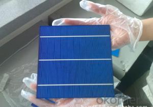


Solar Cell High Quality A Grade Cell Polyrystalline 5v 15.8%
- Ref Price:
-

- Loading Port:
- Shanghai
- Payment Terms:
- TT OR LC
- Min Order Qty:
- 1000 pc
- Supply Capability:
- 100000 pc/month
OKorder Service Pledge
OKorder Financial Service
You Might Also Like


Specifications
hot sale solar cell
1.16.8%~18.25% high efficiency
2.100% checked quality
3.ISO9001/ISO14001/TUV/CE/UL
4.stable performance
We can offer you the best quality products and services, don't miss !
POLY6'(156*156)
Polycrystalline Silicon Solar cell
Physical Characteristics
Dimension: 156mm×156mm±0.5mm
Diagonal: 220mm±0.5mm
Thickness(Si): 200±20 μm
Front(-) Back(+)
Blue anti-reflecting coating (silicon nitride); Aluminum back surface field;
1.5mm wide bus bars; 2.0mm wide soldering pads;
Distance between bus bars: 51mm . Distance between bus bars :51mm .
Electrical Characteristics
Efficiency(%) | 18.00 | 17.80 | 17.60 | 17.40 | 17.20 | 16.80 | 16.60 | 16.40 | 16.20 | 16.00 | 15.80 | 15.60 |
Pmpp(W) | 4.33 | 4.29 | 4.24 | 4.19 | 4.14 | 4.09 | 4.04 | 3.99 | 3.94 | 3.90 | 3.86 | 3.82 |
Umpp(V) | 0.530 | 0.527 | 0.524 | 0.521 | 0.518 | 0.516 | 0.514 | 0.511 | 0.509 | 0.506 | 0.503 | 0.501 |
Impp(A) | 8.159 | 8.126 | 8.081 | 8.035 | 7.990 | 7.938 | 7.876 | 7.813 | 7.754 | 7.698 | 7.642 | 7.586 |
Uoc(V) | 0.633 | 0.631 | 0.628 | 0.625 | 0.623 | 0.620 | 0.618 | 0.617 | 0.615 | 0.613 | 0.611 | 0.609 |
Isc(A) | 8.709 | 8.677 | 8.629 | 8.578 | 8.531 | 8.478 | 8.419 | 8.356 | 8.289 | 8.220 | 8.151 | 8.083 |

MONO5'(125*125mm)165
Monocrystalline silicon solar cell
Physical Characteristics
Dimension: 125mm×125mm±0.5mm
Diagonal: 165mm±0.5mm
Thickness(Si): 200±20 μm
Front(-) Back(+)
Blue anti-reflecting coating(silicon nitride); Aluminum back surface field;
1.6mmwide bus bars; 2.5mm wide soldering pads;
Distance between bus bars: 61mm . Distance between bus bars :61mm .
Electrical Characteristics
Efficiency(%) | 19.40 | 19.20 | 19.00 | 18.80 | 18.60 | 18.40 | 18.20 | 18.00 | 17.80 | 17.60 | 17.40 | 17.20 |
Pmpp(W) | 2.97 | 2.94 | 2.91 | 2.88 | 2.85 | 2.82 | 2.79 | 2.76 | 2.73 | 2.70 | 2.67 | 2.62 |
Umpp(V) | 0.537 | 0.535 | 0.533 | 0.531 | 0.527 | 0.524 | 0.521 | 0.518 | 0.516 | 0.515 | 0.513 | 0.509 |
Impp(A) | 5.531 | 5.495 | 5.460 | 5.424 | 5.408 | 5.382 | 5.355 | 5.328 | 5.291 | 5.243 | 5.195 | 4.147 |
Uoc(V) | 0.637 | 0.637 | 0.636 | 0.635 | 0.633 | 0.630 | 0.629 | 0.629 | 0.628 | 0.626 | 0.626 | 0.625 |
Isc(A) | 5.888 | 5.876 | 5.862 | 5.848 | 5.839 | 5.826 | 5.809 | 5.791 | 5.779 | 5.756 | 5.293 | 5.144 |

FAQ:
Q:How can i get some sample?
A:Yes , if you want order ,sample is not a problem.
Q:How about your solar panel efficency?
A: Our product efficency around 17.25%~18.25%.
Q:What’s the certificate you have got?
A: we have overall product certificate of ISO9001/ISO14001/CE/TUV/UL
- Q:Can solar silicon wafers be used in floating solar panel installations?
- Yes, solar silicon wafers can be used in floating solar panel installations. Floating solar panels typically use photovoltaic cells, which are made of silicon wafers. These wafers are specifically designed to convert sunlight into electricity, making them suitable for floating solar panel systems.
- Q:What is the role of the front contact on a solar silicon wafer?
- The front contact on a solar silicon wafer plays a crucial role in the conversion of sunlight into electricity. It acts as a conductive layer that collects the electrical current generated by the solar cells. Additionally, the front contact helps in reflecting and trapping sunlight, allowing for better absorption and utilization of solar energy. It also protects the underlying layers of the solar cell from external factors such as moisture, dust, and corrosion, thereby ensuring the longevity and efficiency of the solar panel.
- Q:How do solar silicon wafers contribute to the circular economy?
- Solar silicon wafers contribute to the circular economy by promoting sustainable practices throughout their life cycle. Firstly, the production of these wafers involves recycling and reusing silicon materials, reducing the need for extracting new resources. Secondly, solar panels made from these wafers generate renewable energy, reducing dependence on fossil fuels and minimizing greenhouse gas emissions. Moreover, at the end of their life, solar panels can be recycled, with the silicon wafers being recovered and reused, thus closing the material loop and minimizing waste. Overall, solar silicon wafers play a crucial role in transitioning towards a more sustainable and circular economy.
- Q:How is a solar silicon wafer tested for quality control?
- A solar silicon wafer is tested for quality control through various processes, including visual inspection, electrical measurements, and material characterization. Visual inspection involves checking for any physical defects such as cracks, scratches, or impurities on the wafer's surface. Electrical measurements are conducted to assess the wafer's performance, including parameters like resistivity, efficiency, and output power. Material characterization techniques like spectroscopy and microscopy are used to analyze the composition, crystalline structure, and purity of the wafer. These quality control tests ensure that only wafers meeting the desired standards are used in solar cell production.
- Q:What are the different manufacturing methods for solar silicon wafers?
- There are primarily three manufacturing methods for solar silicon wafers: the Czochralski (CZ) method, the Float Zone (FZ) method, and the Multi-Crystalline Silicon (mc-Si) method. The CZ method involves melting high-purity silicon in a crucible and slowly pulling a single crystal from the molten material. The FZ method also melts silicon, but instead of pulling a single crystal, a small seed crystal is dipped into the molten material and then slowly moved upwards, allowing a single crystal to form. The mc-Si method utilizes multiple silicon crystals, which are melted and then casted into blocks, which are later sliced into wafers. Each method has its own advantages and disadvantages, impacting the cost, quality, and efficiency of the resulting solar silicon wafers.
- Q:Can solar silicon wafers be used in other applications besides solar energy?
- Yes, solar silicon wafers can be used in other applications besides solar energy. They are also used in the production of semiconductors, integrated circuits, and various electronic devices. Additionally, they can be utilized in the manufacturing of sensors, batteries, and even medical devices.
- Q:Can solar silicon wafers be used in portable solar panels?
- Yes, solar silicon wafers can be used in portable solar panels. These wafers are commonly used in the production of photovoltaic cells, which generate electricity from sunlight. By incorporating solar silicon wafers into portable solar panels, it allows for the conversion of solar energy into usable electrical energy while maintaining a lightweight and portable design.
- Q:Begged monocrystalline silicon rod is to use what tools and equipment to cut into silicon. What are the most commonly used methods. Loss big? Thank you
- General loss of about 40%, the general thickness of about 190um silicon, cutting seam in 120um
- Q:What is the silicon wafer, the specific definition of what?
- Silicon wafer, which is an important material for making integrated circuits, can be made into various semiconductor devices by photolithography and ion implantation.
- Q:From raw materials to finished products processing and production of the main links? Construction technology? Key issues of safety in production? What security measures are generally taken?
- Another reason is that CZ is easier to produce large size single crystal silicon rods than FZ method. At present, using the method of CZ CZ main equipment: CZ growth furnace growth furnace by CZ components can be divided into four parts: (1) the furnace body comprises a quartz crucible, graphite crucible, heating and insulating element in the furnace wall (2) crystal and crucible for rotary mechanism: including seed chuck, hanging and pulled the rotating element (3) atmosphere pressure control: including gas flow control, vacuum system and pressure control valve (4) control system: including the detection sensor and computer control system processing: charging, melting, necking, shoulder growth, growth, growth and diameter growth of the tail (1) charging: the polysilicon raw materials and impurities in the quartz crucible, the type of impurity depends on the N or P type resistance. Boron, phosphorus, antimony, arsenic. (2): after the melting quartz crucible for polysilicon feedstock after long crystal furnace must be closed and vacuum filling in high purity argon to maintain a certain pressure range, and then open the graphite heater power supply, heating to the melting temperature (1420 DEG C) above, the polysilicon raw material melting. (3) necking growth: when the temperature of the silicon melt is stable, the seed is slowly immersed in the silicon melt. Because of the thermal stress in the contact between the seed and the silicon melt, the seeds will be dislocation, which must be used to reduce the growth of the crystal. Necking is the seed growth will rapidly upward, the seed crystal grows to a certain size of the reduced diameter (4-6mm) due to the dislocation line and growth axis into a corner, as long as the neck is long enough, the dislocation can grow the crystal surface, zero crystal dislocation.
1. Manufacturer Overview |
|
|---|---|
| Location | |
| Year Established | |
| Annual Output Value | |
| Main Markets | |
| Company Certifications | |
2. Manufacturer Certificates |
|
|---|---|
| a) Certification Name | |
| Range | |
| Reference | |
| Validity Period | |
3. Manufacturer Capability |
|
|---|---|
| a)Trade Capacity | |
| Nearest Port | |
| Export Percentage | |
| No.of Employees in Trade Department | |
| Language Spoken: | |
| b)Factory Information | |
| Factory Size: | |
| No. of Production Lines | |
| Contract Manufacturing | |
| Product Price Range | |
Send your message to us
Solar Cell High Quality A Grade Cell Polyrystalline 5v 15.8%
- Ref Price:
-
- Loading Port:
- Shanghai
- Payment Terms:
- TT OR LC
- Min Order Qty:
- 1000 pc
- Supply Capability:
- 100000 pc/month
OKorder Service Pledge
OKorder Financial Service
Similar products


New products
Hot products


Hot Searches
Related keywords

