Solar Cell High Quality A Grade Cell Monorystalline 5v 17.8%
- Ref Price:
-

- Loading Port:
- Shanghai
- Payment Terms:
- TT OR LC
- Min Order Qty:
- 1000 pc
- Supply Capability:
- 100000 pc/month
OKorder Service Pledge
OKorder Financial Service
You Might Also Like


Specifications
hot sale solar cell
1.16.8%~18.25% high efficiency
2.100% checked quality
3.ISO9001/ISO14001/TUV/CE/UL
4.stable performance
We can offer you the best quality products and services, don't miss !
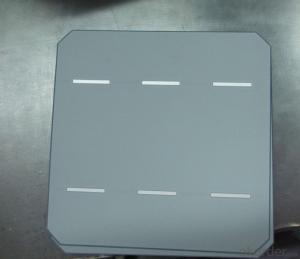
POLY6'(156*156)
Polycrystalline Silicon Solar cell
Physical Characteristics
Dimension: 156mm×156mm±0.5mm
Diagonal: 220mm±0.5mm
Thickness(Si): 200±20 μm
Front(-) Back(+)
Blue anti-reflecting coating (silicon nitride); Aluminum back surface field;
1.5mm wide bus bars; 2.0mm wide soldering pads;
Distance between bus bars: 51mm . Distance between bus bars :51mm .
Electrical Characteristics
Efficiency(%) | 18.00 | 17.80 | 17.60 | 17.40 | 17.20 | 16.80 | 16.60 | 16.40 | 16.20 | 16.00 | 15.80 | 15.60 |
Pmpp(W) | 4.33 | 4.29 | 4.24 | 4.19 | 4.14 | 4.09 | 4.04 | 3.99 | 3.94 | 3.90 | 3.86 | 3.82 |
Umpp(V) | 0.530 | 0.527 | 0.524 | 0.521 | 0.518 | 0.516 | 0.514 | 0.511 | 0.509 | 0.506 | 0.503 | 0.501 |
Impp(A) | 8.159 | 8.126 | 8.081 | 8.035 | 7.990 | 7.938 | 7.876 | 7.813 | 7.754 | 7.698 | 7.642 | 7.586 |
Uoc(V) | 0.633 | 0.631 | 0.628 | 0.625 | 0.623 | 0.620 | 0.618 | 0.617 | 0.615 | 0.613 | 0.611 | 0.609 |
Isc(A) | 8.709 | 8.677 | 8.629 | 8.578 | 8.531 | 8.478 | 8.419 | 8.356 | 8.289 | 8.220 | 8.151 | 8.083 |

MONO5'(125*125mm)165
Monocrystalline silicon solar cell
Physical Characteristics
Dimension: 125mm×125mm±0.5mm
Diagonal: 165mm±0.5mm
Thickness(Si): 200±20 μm
Front(-) Back(+)
Blue anti-reflecting coating(silicon nitride); Aluminum back surface field;
1.6mmwide bus bars; 2.5mm wide soldering pads;
Distance between bus bars: 61mm . Distance between bus bars :61mm .
Electrical Characteristics
Efficiency(%) | 19.40 | 19.20 | 19.00 | 18.80 | 18.60 | 18.40 | 18.20 | 18.00 | 17.80 | 17.60 | 17.40 | 17.20 |
Pmpp(W) | 2.97 | 2.94 | 2.91 | 2.88 | 2.85 | 2.82 | 2.79 | 2.76 | 2.73 | 2.70 | 2.67 | 2.62 |
Umpp(V) | 0.537 | 0.535 | 0.533 | 0.531 | 0.527 | 0.524 | 0.521 | 0.518 | 0.516 | 0.515 | 0.513 | 0.509 |
Impp(A) | 5.531 | 5.495 | 5.460 | 5.424 | 5.408 | 5.382 | 5.355 | 5.328 | 5.291 | 5.243 | 5.195 | 4.147 |
Uoc(V) | 0.637 | 0.637 | 0.636 | 0.635 | 0.633 | 0.630 | 0.629 | 0.629 | 0.628 | 0.626 | 0.626 | 0.625 |
Isc(A) | 5.888 | 5.876 | 5.862 | 5.848 | 5.839 | 5.826 | 5.809 | 5.791 | 5.779 | 5.756 | 5.293 | 5.144 |

FAQ:
Q:How can i get some sample?
A:Yes , if you want order ,sample is not a problem.
Q:How about your solar panel efficency?
A: Our product efficency around 17.25%~18.25%.
Q:What’s the certificate you have got?
A: we have overall product certificate of ISO9001/ISO14001/CE/TUV/UL
- Q:How is the doping level of a solar silicon wafer controlled?
- The doping level of a solar silicon wafer is controlled through a process known as doping. Doping involves the intentional introduction of impurities into the silicon crystal lattice to alter its electrical properties. This is achieved by diffusing specific atoms, such as boron or phosphorus, into the silicon wafer during its manufacturing process. The concentration of these impurities determines the doping level, with higher concentrations leading to higher levels of doping. By carefully controlling the amount and distribution of these impurities, manufacturers can achieve the desired doping level to optimize the solar wafer's electrical conductivity and performance.
- Q:Are solar silicon wafers affected by voltage fluctuations?
- Yes, solar silicon wafers can be affected by voltage fluctuations. Voltage fluctuations can impact the overall performance and efficiency of solar panels, potentially leading to reduced power output. It is important to maintain a stable and consistent voltage supply to optimize the performance and lifespan of solar silicon wafers.
- Q:Can solar silicon wafers be used in off-grid solar applications?
- Yes, solar silicon wafers can be used in off-grid solar applications. These wafers are commonly used in the production of solar panels, which can generate electricity from sunlight. Off-grid solar systems are designed to operate independently of the traditional power grid, making them a suitable application for solar silicon wafers as they can harness solar energy to power various appliances and devices in remote locations.
- Q:Can solar silicon wafers be used in art installations?
- Yes, solar silicon wafers can be used in art installations. These wafers can be creatively incorporated into various artistic designs to add a unique and sustainable element to the installation.
- Q:What is the role of surface passivation in solar silicon wafers?
- The role of surface passivation in solar silicon wafers is to reduce or eliminate surface recombination, which is the process by which charge carriers (electrons and holes) recombine at the surface of the wafer, leading to a loss of efficiency in solar cell performance. Passivation involves applying a thin layer of material, such as silicon nitride or aluminum oxide, to the surface of the wafer to create a barrier that prevents the recombination of charge carriers. This helps to improve the efficiency and overall performance of the solar cell by reducing the loss of generated electricity due to surface recombination.
- Q:What is the role of front contacts on solar silicon wafers?
- The role of front contacts on solar silicon wafers is to collect and extract the generated electricity from the solar cells. These contacts are typically made of metal fingers or grids that are placed on the front surface of the solar cell. They enable the flow of current and help in minimizing the resistance and losses, ensuring efficient electricity production from the solar panel.
- Q:How are solar silicon wafers tested for thermal properties?
- Solar silicon wafers are tested for thermal properties through various methods such as thermal conductivity measurements, thermoreflectance imaging, and infrared thermography. These techniques allow the determination of the wafer's ability to conduct heat efficiently, detect any defects or irregularities, and assess its overall thermal performance.
- Q:Can solar silicon wafers be used in solar-powered recreational facilities?
- Yes, solar silicon wafers can be used in solar-powered recreational facilities. These wafers are commonly used in the production of solar panels, which generate electricity from sunlight. Solar-powered recreational facilities can benefit from this technology by harnessing solar energy to power various amenities such as lighting, heating, and cooling systems.
- Q:How long do solar silicon wafers last?
- Solar silicon wafers have a long lifespan and can last for several decades. With proper maintenance and care, they can continue to generate electricity efficiently for at least 25 to 30 years.
- Q:How are solar silicon wafers affected by surface recombination velocity?
- Solar silicon wafers are significantly affected by surface recombination velocity. High surface recombination velocities can lead to the loss of majority carriers near the surface, reducing the efficiency of solar cells. This results in a decrease in the overall conversion of sunlight into electricity. Therefore, minimizing surface recombination velocity is crucial to enhance the performance of solar silicon wafers and improve the efficiency of solar cells.
1. Manufacturer Overview |
|
|---|---|
| Location | |
| Year Established | |
| Annual Output Value | |
| Main Markets | |
| Company Certifications | |
2. Manufacturer Certificates |
|
|---|---|
| a) Certification Name | |
| Range | |
| Reference | |
| Validity Period | |
3. Manufacturer Capability |
|
|---|---|
| a)Trade Capacity | |
| Nearest Port | |
| Export Percentage | |
| No.of Employees in Trade Department | |
| Language Spoken: | |
| b)Factory Information | |
| Factory Size: | |
| No. of Production Lines | |
| Contract Manufacturing | |
| Product Price Range | |
Send your message to us
Solar Cell High Quality A Grade Cell Monorystalline 5v 17.8%
- Ref Price:
-
- Loading Port:
- Shanghai
- Payment Terms:
- TT OR LC
- Min Order Qty:
- 1000 pc
- Supply Capability:
- 100000 pc/month
OKorder Service Pledge
OKorder Financial Service
Similar products


New products
Hot products


Hot Searches
Related keywords

